Color el display and method for producing the same

a color el and display technology, applied in the direction of discharge tube luminescnet screens, discharge tube/lamp details, coatings, etc., can solve the problems of insufficient response to high-speed pixel signals, large amount of power consumption, narrow viewing angle, etc., to improve the aperture ratio of active matrix type organic el displays, the effect of good color purity

Active Publication Date: 2008-06-05
TOPPAN PRINTING CO LTD
View PDF12 Cites 3988 Cited by
  • Summary
  • Abstract
  • Description
  • Claims
  • Application Information

AI Technical Summary

Benefits of technology

[0010]A purpose of the present invention is to create active matrix type organic EL displays with a simple structure having color filters, and to provide organic EL displays of high quality having good color purity. In addition, another purpose thereof is to improve the aperture ratio of active matrix type organic EL displays, thereby reducing load imposed on the organic EL layer. One aspect of the invention is a color EL display characterized in that at least color filters, a thin film transistor circuit, an organic EL layer, and a common electrode are built in this order on a transparent substrate.

Problems solved by technology

However, liquid crystal displays have such problems as a narrow viewing angle and insufficient response to high-speed pixel signals, and plasma displays have such problems as a large amount of power consumption and many technical subjects to be solved for increasing to a larger size than current one.
In a simple matrix type display, the organic EL layer is required to perform very high-brightness emission in a selected moment, thus there are such problems that the organic EL layer degrades severely and wiring resistance results in large voltage drop.
However, in active matrix type organic EL displays based on selective coating of R, G and B light-emitting layers, there is such a problem that color purity is insufficient, that is, green is whitish and red is yellowish.
In addition, there is such a problem that a “white EL+color filter” system and a “blue EL+color conversion layer” system can be applied only to simple matrix type displays.
However, in the method, it is necessary to connect the TFT and the organic EL by means of a via hole, to result in a complex construction and low reliability.

Method used


Image

  • Color el display and method for producing the same
  • Color el display and method for producing the same
  • Color el display and method for producing the same

Examples


example 1

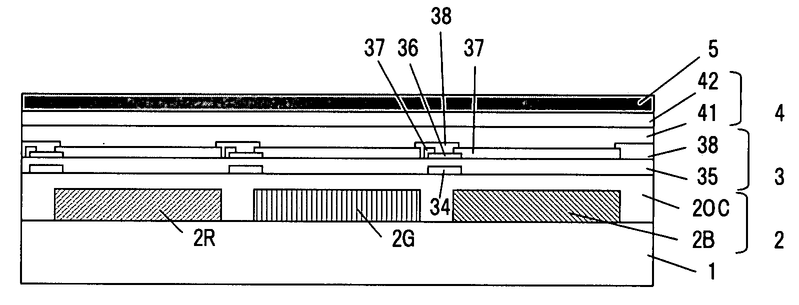
[0064]As a transparent substrate 1, glass was used, on which color filters 2 were formed through pigment-dispersed resist coating, exposure, development and burning (FIG. 11A). 2R denotes red, 2G denotes green, 2B denotes blue, and 2OC denotes over coating. Here, for the over coating, neither exposure nor development is necessary. The burning temperature was 220° C.

[0065]Next, ITO was formed into a film as the first electrode layer 31 including the gate electrode G1 and capacitor electrode C, by reactive sputtering (room temperature, DC sputtering) under an Ar+O2 gas using ITO as a target, which was patterned through photoresist coating, exposure, development, wet etching with hydrochloric acid, and resist strip (FIG. 11B). Then, each of SiON as the first insulating layer 32 and InGaZn oxide as the first semiconductor layer 33 was formed into a film continuously, by reactive sputtering (room temperature, RF sputtering) under an Ar+O2+N2 gas using SiN as a target, and by reactive spu...

example 2

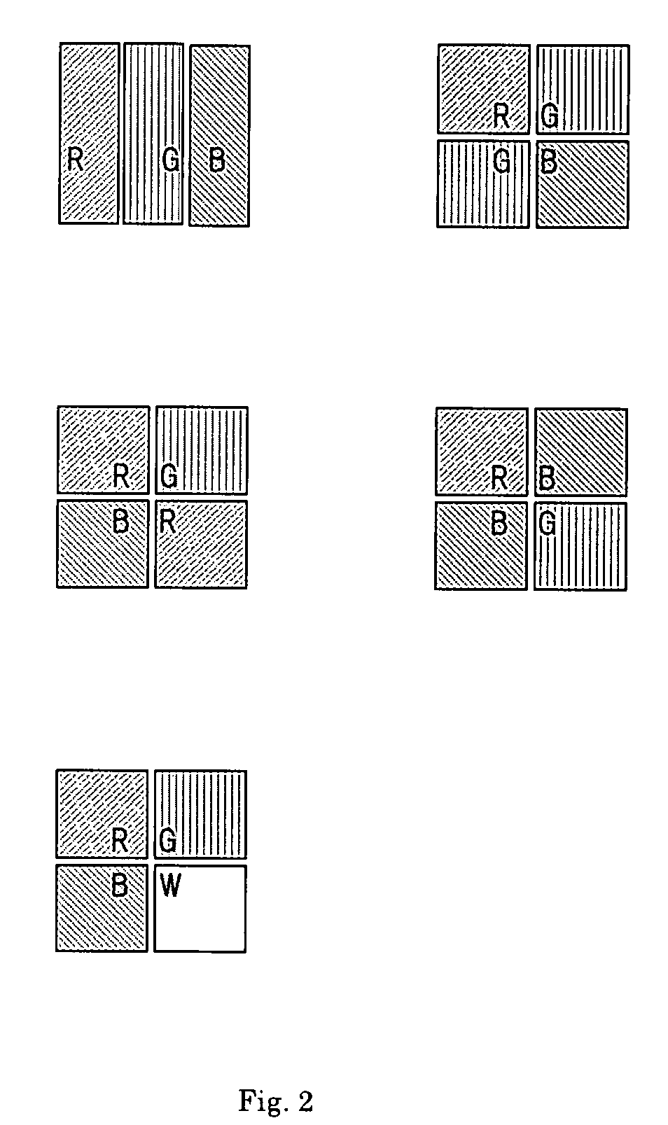
[0069]As the transparent substrate 1, glass was used, on which color filters 2 were formed through pigment-dispersed resist coating, exposure, development, burning, fluorescent coloring material-containing resist coating, exposure, development and burning (FIG. 15A). 2R, 2G and 2B denote red, green and blue band-limiting filters, and 2RR and 2GG denote red and green color conversion filters, respectively, and 2OC is an over coating. Here, for the over coating, neither exposure nor development is necessary. The burning temperature was 200° C.

[0070]Next, ITO was formed into a film as a first electrode layer 31 including the gate electrodes G1 and G2 by reactive sputtering (room temperature, DC sputtering) under an Ar+O2 gas using ITO as a target, which was patterned through photoresist coating, exposure, development, wet etching with hydrochloric acid, and resist strip (FIG. 15B). Then, each of SiON as the first insulating layer 32 and InGaZnMg oxide as the first semiconductor layer 3...

example 3

[0074]A color EL display was produced in the same process as in Example 2, except that, as the light-emitting layer 42, a polyolefin-based material was used as a blue light-emitting layer 42B in place of a white light-emitting layer 42W. The process of forming a TFT circuit and all the subsequent processes were performed at 200° C. or less. The color EL display thus produced could perform display having good color purity and brightness due to a large aperture ratio, when being viewed from the transparent substrate 1 side.


PUM

PropertyMeasurementUnit
temperatureaaaaaaaaaa
wavelength rangeaaaaaaaaaa
transmittanceaaaaaaaaaa

Abstract

One embodiment of the present invention is a color EL display characterized in that at least color filters, a thin film transistor circuit, an organic EL layer, and a common electrode are laminated in this order on a transparent substrate. Another embodiment of the invention is a method for producing a color EL display comprising the steps of forming color filters or a transparent substrate; forming a thin film transistor circuit; forming an organic EL layer; and forming a common electrode, wherein process temperatures of the steps of forming the thin film transistor circuit and subsequent steps are 200° C. or less.

Description

CROSS REFERENCE[0001]This application claims priority to Japanese application number 2006-326742, filed on Dec. 4, 2006, which is incorporated by reference.BACKGROUND OF THE INVENTION[0002]1. Field of the Invention[0003]The present invention relates to an organic EL display, which is one kind of flat-panel displays.[0004]2. Description of the Related Art[0005]As flat-panel displays, liquid crystal displays and plasma displays are commercialized. However, liquid crystal displays have such problems as a narrow viewing angle and insufficient response to high-speed pixel signals, and plasma displays have such problems as a large amount of power consumption and many technical subjects to be solved for increasing to a larger size than current one.[0006]What is drawing attention recently in contrast to these is an organic electroluminescence display (organic EL display) that uses organic light-emitting materials. By using organic compounds as light-emitting materials, it is expected as a d...

Claims


Application Information

Patent Timeline
Patent Type & Authority Applications(United States)
IPC IPC(8): H01L51/54C09K11/00
CPCH01L27/322H10K59/38
Inventor ISHIZAKI, MAMORUSEKINE, NORIMASAITO, MANABUKITAZUME, EIICHI
Owner TOPPAN PRINTING CO LTD
Why Eureka
Try Eureka