Environmental Protection Coating System and Method

a technology of environmental protection and coating system, applied in the direction of superimposed coating process, liquid/solution decomposition chemical coating, semiconductor/solid-state device details, etc., can solve the problems of particulates or other contaminants, easy to damage the circuit board assembly, etc., to eliminate or minimize the occurrence of tin whiskers, improve electrical performance, mechanical protection and environmental protection, and reduce the effect of tin whiskers

Active Publication Date: 2008-08-07
RAYTHEON CO
View PDF24 Cites 44 Cited by
  • Summary
  • Abstract
  • Description
  • Claims
  • Application Information

AI Technical Summary

Benefits of technology

[0005]In another embodiment of the disclosure, a structure consisting of an environmentally sealed domed lid enclosure is placed locally over the active or passive device region which is sensitive to dielectric loading. The localized enclosure allows utilization of a relatively thick environmental coating to provide improved electrical performance, mechanical protection, and environmental protection. The relatively thick environmental coating described in this disclosure may also eliminate or minimize the occurrence of tin whiskers. The thick environmental coating may be utilized independently or in conjunction with the lid for lower frequency circuit board operation where dielectric loading is a second order concern.
[0006]Embodiments of the disclosure may provide numerous technical advantages. Some, none, or all embodiments may benefit from the below described advantages. According to one embodiment, an environmental protection coating system may be provided for discrete electrical components or other assembly level features of a circuit board assembly during the assembly level phase of production. These discrete electrical components or other assembly level features may render the circuit board assembly susceptible to moisture attack, particulates or other contaminants. The environmental protection coating system of the present disclosure includes a dielectric layer made of a dielectric material that may be applied in a relatively consistent thickness to protect the discrete electrical components or other assembly level features from moisture or other harmful contaminants with relatively little impact on circuit performance.

Problems solved by technology
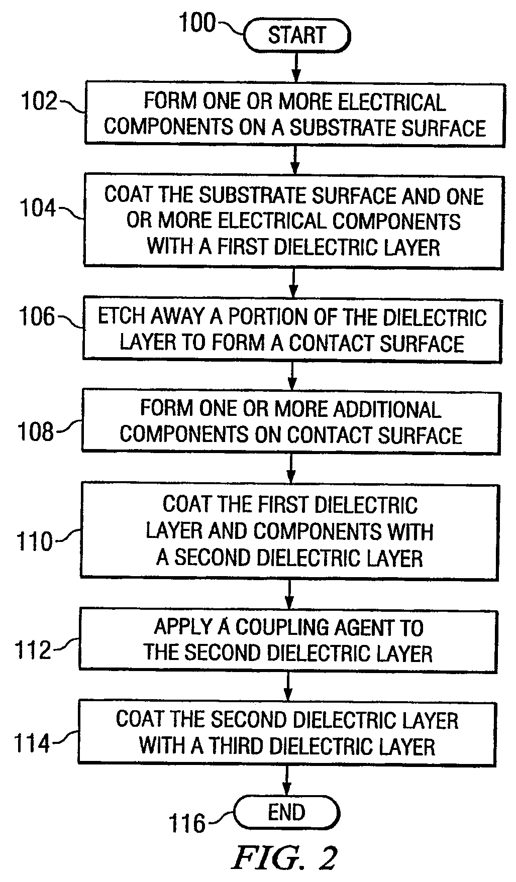
These discrete electrical components or other assembly level features may render the circuit board assembly susceptible to moisture attack, particulates or other contaminants.

Method used


Image

  • Environmental Protection Coating System and Method
  • Environmental Protection Coating System and Method
  • Environmental Protection Coating System and Method

Examples


embodiment 1

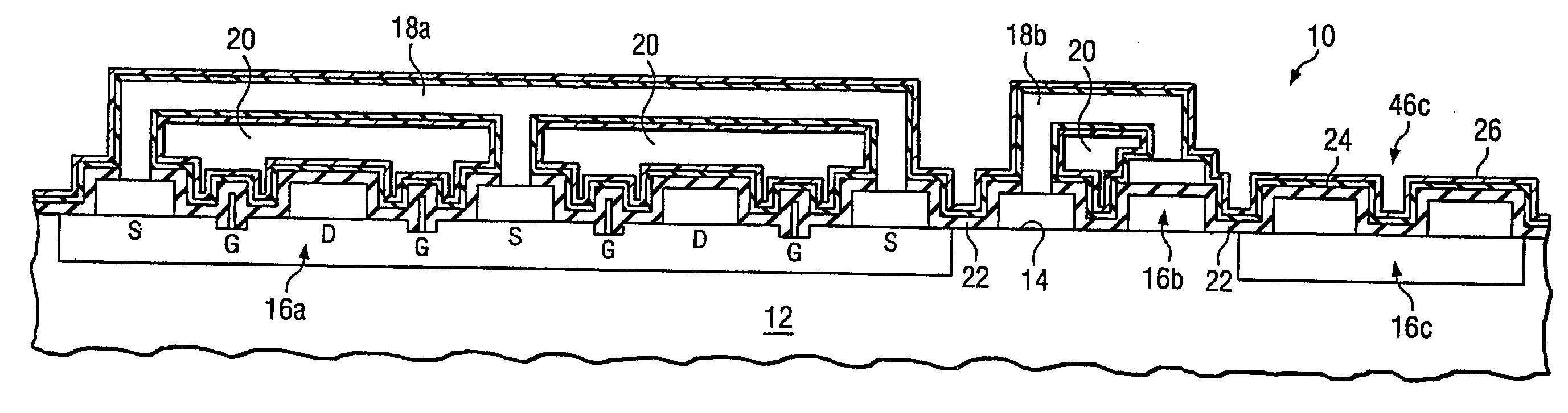
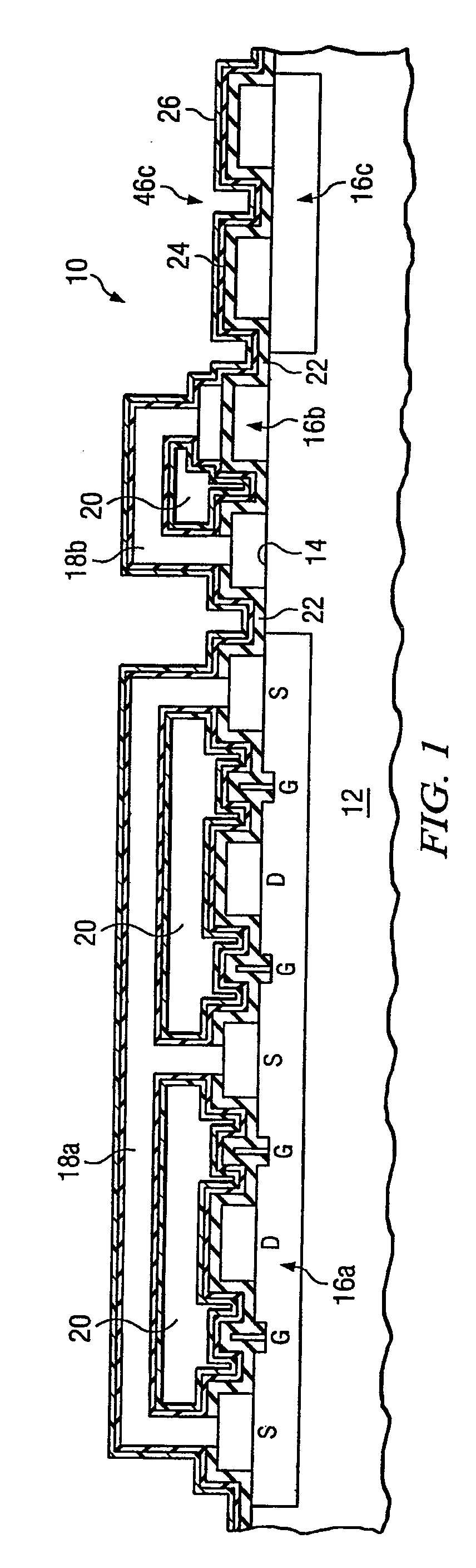
[0037 of FIG. 3 utilizes only a first protective dielectric layer 22 made of alumina. Embodiment 1 may provide enhanced electrical performance due to minimal internode capacitance of a single dielectric layer while providing electrical, physical and environmental protection of the source region S, gate region G, and drain region D of transistor 16a of FIG. 1. Embodiment 1 may also provide enhanced electrical performance over known materials, such as silicon-nitride or silicon-dioxide in both hermetic and non-hermetic environments. Enhanced performance may be provided since a thinner dielectric than conventional silicon-nitride or silicon-dioxide can be utilized. Embodiment 1 may also be desirable in environments where partial control of temperature and or humidity is provided at the system level such that conditions are provided that minimize or eliminate water condensation on active circuitry and / or minimize or eliminate high temperature and humidity exposure of active circuitry fo...

embodiment 2

[0038 provides first 22 and second 24 protective dielectric layers formed of alumina. The second protective dielectric layer 24 covers unprotected additional components 18 such as air bridges and thick metal lines, which may be formed after the first protective dielectric layer 22 is applied. Embodiment 2 may also be desirable in hermetic or less severe humidity environments where protection against conductive or corrosive solid, liquid or gases materials may be present.

[0039]Embodiments 3 and 4 provide a third dielectric layer 26 that may be formed of silica or parylene F, parylene HT®, or other fluorinated parylene-like film as described above. The third dielectric layer 26 formed of silica or parylene F, parylene HT®, or other fluorinated parylene-like films protects the first 22 and / or second 24 protective dielectric layers from high humidity, extended humidity and / or condensed moisture which may break down the first 22 and / or second 24 protective dielectric layers 24 and expose...


PUM

PropertyMeasurementUnit
thicknessaaaaaaaaaa
thicknessaaaaaaaaaa
wetting angleaaaaaaaaaa

Abstract

According to one embodiment of the disclosure, an environmental protection coating comprises a circuit assembly having a first protective dielectric layer and a second dielectric layer. The circuit assembly has an outer surface on which a plurality of discrete electrical components are attached. The first protective dielectric layer overlays the circuit assembly. The second dielectric layer overlays the first protective dielectric layer and is made of a dielectric material having modulus of elasticity less than 3.5 Giga-Pascal (GPa), dielectric constant less than 2.7, dielectric loss less than 0.008, breakdown voltage strength in excess of 2 million volts/centimeter (MV/cm), temperature stability to 3000 Celsius, defect densities less than 0.5/centimeter, pinhole free in films greater than 50 Angstroms, capable of being deposited conformally over and under 3D structures with thickness uniformity less than or equal to 10%.

Description

TECHNICAL FIELD OF THE DISCLOSURE[0001]This disclosure relates generally to environmental protection coatings, and more particularly, to an environmental protection coating system and method of manufacturing the same.BACKGROUND OF THE DISCLOSURE[0002]Circuit devices having electrical components that are integrally formed on a substrate and circuit board assemblies comprised of active and passive devices have enjoyed wide acceptance due to the wide variety of uses they may provide. Uses for these circuit devices and circuit board assemblies may include applications where operation in a protected environment is not readily available, is costly and / or limits system performance. For such applications, passivation techniques may be employed such that the electrical performance of the components are improved and the components of the circuit device may be protected against harmful contaminants such as moisture, humidity, particulates, or ionic impurities, such as those produced from sodiu...

Claims


Application Information

Patent Timeline
Patent Type & Authority Applications(United States)
IPC IPC(8): H05K3/30H05K1/00H05K3/00
CPCH01L23/3192Y10T29/49146H01L24/83H01L2224/73265H01L2224/83801H01L2224/83851H01L2224/8592H01L2924/01004H01L2924/0781H01L2924/1423H01L2924/19041H05K3/284H05K2201/0179H05K2201/0195H05K2203/1322H01L2924/01019H01L23/4821Y10T29/49124Y10T29/49982Y10T29/49155H01L2924/1305H01L2924/00011H01L2224/293H01L2224/2929H01L2224/48137H01L2924/3512H01L2924/00H01L2224/29075H01L2924/00014H01L2924/14H01L2224/45014H01L21/76832H01L21/76834H01L21/7682H01L2924/206
Inventor BEDINGER, JOHN M.MOORE, MICHAEL A.
Owner RAYTHEON CO
Why Eureka
Try Eureka