Organic thin film transistor having surface-modified carbon nanotubes

a carbon nanotube, organic technology, applied in the direction of thermoelectric devices, solid-state devices, nanoinformatics, etc., can solve the problems of relatively high driving voltage, relatively high threshold voltage of organic thin film transistors, and relatively low charge carrier mobility

Active Publication Date: 2008-08-14
SAMSUNG ELECTRONICS CO LTD
View PDF10 Cites 55 Cited by
  • Summary
  • Abstract
  • Description
  • Claims
  • Application Information

AI Technical Summary

Benefits of technology

[0007]An organic thin film transistor according to example embodiments may have a structure comprising an organic semiconductor layer and further comprising one or more gate electrodes, one or more source / drain electrodes, and / or a gate insulating layer provided on a substrate, wherein the organic semiconductor layer may comprise surface-modified carbon nanotubes and an electrically-conductive polymer. The organic thin film transistor may further comprise data lines and / or banks.

Problems solved by technology

As a result, the relatively high contact resistance may render the injection of carriers ineffective, thus resulting in relatively low charge carrier mobility, relatively high driving voltage, and relatively high threshold voltage for the organic thin film transistors.

Method used


Image

  • Organic thin film transistor having surface-modified carbon nanotubes
  • Organic thin film transistor having surface-modified carbon nanotubes
  • Organic thin film transistor having surface-modified carbon nanotubes

Examples


example 4

Preparative Example 4

Introduction of Oxirane Group into Surfaces of Carbon Nanotubes

[0056]40 mg of the carbon nanotubes surface-modified with an acetyl chloride group, which were prepared in Preparative Example 3, were dispersed in 20 ml of chloroform by sonication for 30 minutes. 4 ml of pyridine and 1 ml of glycidol were sequentially added to the dispersion. The mixture was allowed to react with stirring under refluxing conditions for 48 hours. After completion of the reaction, the reaction mixture was washed several times with methanol to remove unreacted glycidol, and the remaining black solid was dried under reduced pressure at room temperature to yield carbon nanotubes whose surfaces were modified with a glycidyl ether group.

example 5

Preparative Example 5

Introduction of Anhydride Group into Surfaces of Carbon Nanotubes

[0057]40 mg of the carbon nanotubes surface-modified with an acetyl chloride group, which were prepared in Preparative Example 3, were dispersed in 2 ml of dimethylformamide by sonication. 10 ml of pyridine and 2 g of dimethyl 4-hydroxyphthalate were sequentially added to the dispersion. The mixture was allowed to react at 70° C. for about 18 hours. After completion of the reaction, the reaction mixture was washed several times with distilled water. 20 ml of acetone and 10 ml of a solution of sodium hydroxide (0.2 g) in distilled water were sequentially added to the remaining black solid. The mixture was allowed to react with stirring at 60° C. for about 18 hours. After completion of the reaction, the reaction mixture was washed several times with a dilute aqueous hydrochloric acid solution, distilled water, and ethyl acetate, and dried under reduced pressure at room temperature. The dried solid wa...

example 1

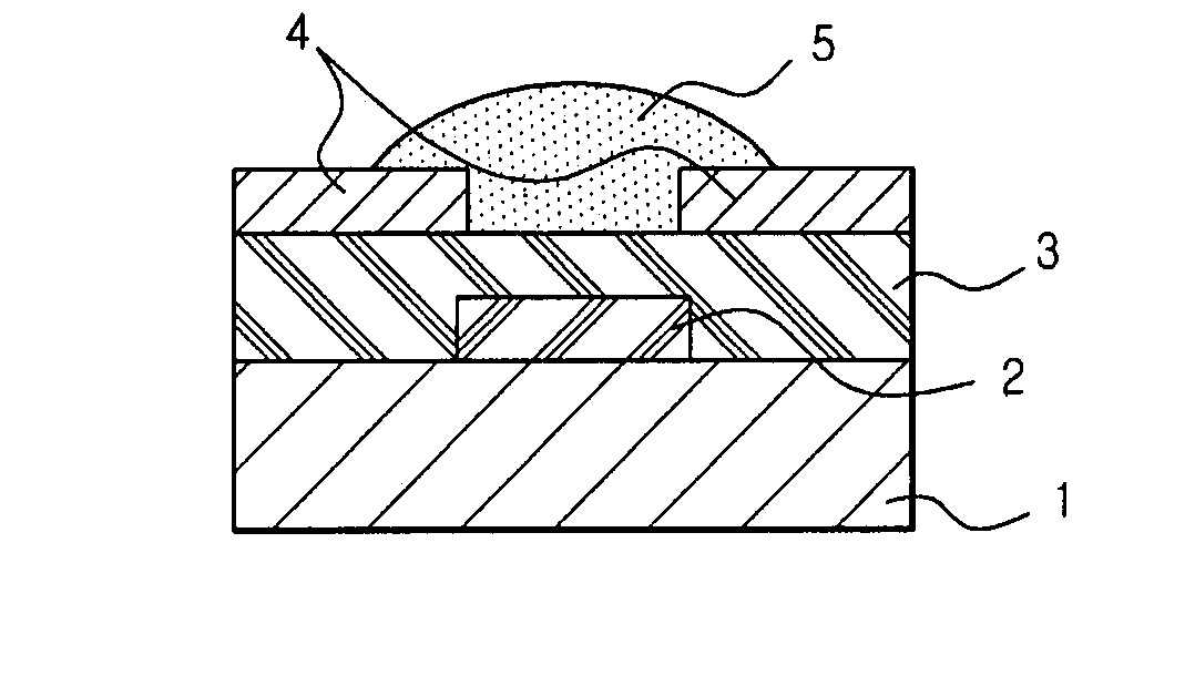
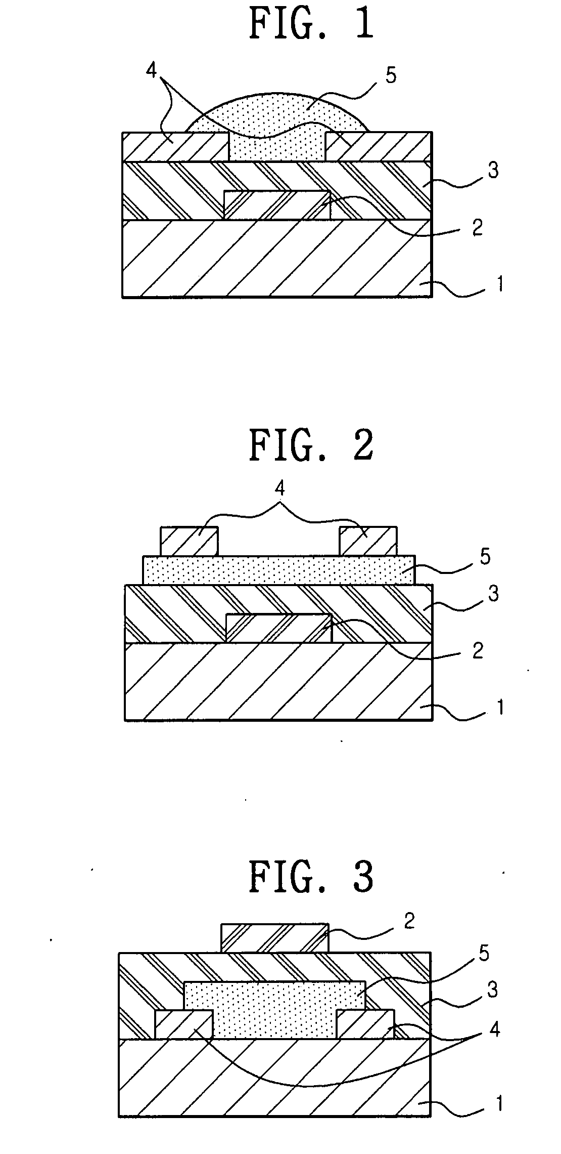
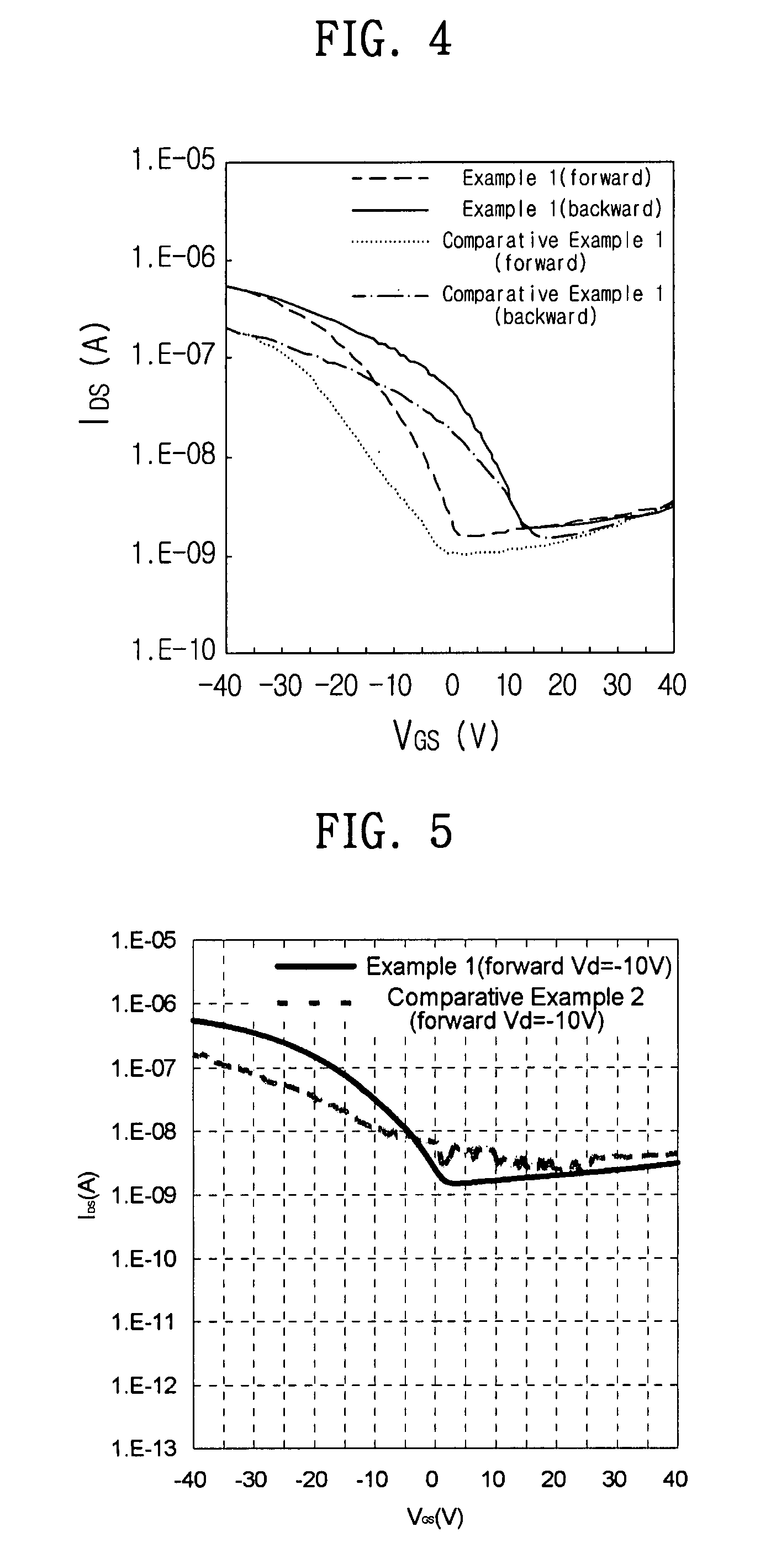
[0058]Polythiophene-thiazole (weight average molecular weight: 15,000) was dissolved in chlorobenzene or chloroform to obtain a polymer solution (1 mg / mL). The carbon nanotubes surface-modified with an oxirane group, which were prepared in Preparative Example 4, were dispersed in a mixed solvent of dimethylformamide and chloroform to obtain a solution of the carbon nanotubes (1 mg / ML). The polymer solution was mixed with the solution of the carbon nanotubes in a weight ratio of 1:1 to prepare a solution for the formation of an organic semiconductor layer 5.

[0059]Aluminum (Al) was deposited to a thickness of 1,000 Å on a clean glass substrate 1 by sputtering to form a gate electrode 2. An organic-inorganic hybrid insulating material was applied by spin casting and dried at 200° C. for 2 hours to form a 7,000 Å-thick gate insulating layer 3. Gold (Au) was deposited to a thickness of 700 Å on the gate insulating layer by thermal evaporation to form source / drain electrodes 4. The soluti...


PUM

PropertyMeasurementUnit
thicknessaaaaaaaaaa
sizeaaaaaaaaaa
temperatureaaaaaaaaaa

Abstract

An organic thin film transistor may comprise an organic semiconductor layer having surface-modified carbon nanotubes and an electrically-conductive polymer. The surfaces of the carbon nanotubes may be modified with curable functional groups, comprising oxirane groups and anhydride groups. A room-temperature solution process may be used to provide a relatively uniform and relatively highly-adhesive organic semiconductor layer in a simple and economical manner. Additionally, the organic thin film transistor having the organic semiconductor layer may have relatively high charge carrier mobility and relatively low threshold voltage.

Description

BACKGROUND OF THE INVENTION[0001]This non-provisional application claims priority under 35 U.S.C. § 119(a) to Korean Patent Application No. 10-2006-0119799, filed on Nov. 30, 2006 in the Korean Intellectual Property Office (KIPO), the entire contents of which are incorporated herein by reference.TECHNICAL FIELD[0002]Example embodiments relate to a thin film transistor structure having an organic semiconductor layer.DESCRIPTION OF THE RELATED ART[0003]Increased interest has been generated regarding organic semiconductors since polyacetylene, as a conjugated organic polymer, was shown to exhibit semiconductor characteristics. As a result, organic semiconductors have been researched for a wide variety of applications (e.g., functional electronic devices and optical devices) because of their relative ease of molding into fibers and films, improved flexibility, relatively high conductivity, and / or relatively low production costs. Organic thin film transistors have especially been the sub...

Claims


Application Information

Patent Timeline
Patent Type & Authority Applications(United States)
IPC IPC(8): H01L51/10
CPCB82Y10/00H01L51/0036H01L51/0043H01L51/0566H01L51/0541H01L51/0545H01L51/0049Y10S977/745H10K85/225H10K85/151H10K85/113H10K10/464H10K10/488H10K10/466
Inventor HAN, KOOK MININ, KYU YEOLPARK, JONG JINMOON, HYUN SIKLEE, SANG YOON
Owner SAMSUNG ELECTRONICS CO LTD
Why Eureka
Try Eureka