Eureka AIR delivers breakthrough ideas for toughest innovation challenges, trusted by R&D personnel around the world.

Method of forming a crosslinked poly(arylene ether) film, and film formed thereby

a crosslinked poly(arylene ether) and film technology, applied in the field of microelectronics, can solve the problems of reducing the reliability of data transport, increasing the delay of signal, and comparatively reducing the heat resistan

Inactive Publication Date: 2008-08-14
SABIC INNOVATIVE PLASTICS IP BV
View PDF19 Cites 6 Cited by
  • Summary
  • Abstract
  • Description
  • Claims
  • Application Information

AI Technical Summary

Benefits of technology

[0004]The above-described and other drawbacks are alleviated by a method of preparing a crosslinked poly(arylene ether) film, comprising: forming a poly(arylene ether) film from a composition comprising a poly(arylene ether) having an intrinsic viscosity of at least 0.2...

Problems solved by technology

These twin factors cause inductive cross-talk and capacitive effects that decrease the reliability of data transport.
Furthermore, higher circuit density results in an increase in the signal delay such that it is the main contributor to the overall signal delay time for sub-micron size devices.
However, it has comparatively lower heat resistance so it typically cannot withstand the multiple soldering operations used in microelectronic fabrication.
However, thermal and thermochemical curing both require elevated temperatures and extended processing times, and the resulting crosslinked films are often brittle.
However, the use of ionizing radiation typically requires the handling of radioactive sources, and, like thermal curing, it typically requires extended processing times.

Method used


Image

  • Method of forming a crosslinked poly(arylene ether) film, and film formed thereby
  • Method of forming a crosslinked poly(arylene ether) film, and film formed thereby
  • Method of forming a crosslinked poly(arylene ether) film, and film formed thereby

Examples


examples 1-4

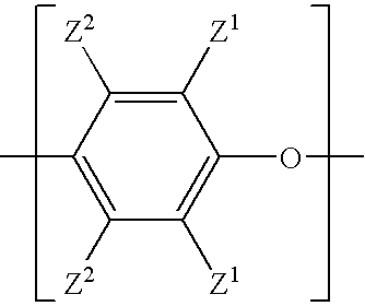
[0039]Four poly(arylene ether) copolymers, designated “APPExx” where the numbered suffix represents the weight percent of 2-allyl-6-methylphenol in the monomer mixture (for example, “APPE10” refers to a copolymer prepared from monomer comprising 10 weight percent), were prepared by oxidative copolymerization of 2,6-dimethylphenol and 2-allyl-6-methylphenol using the following procedure. Nitrogen was flowed through a reactor maintained at 25° C. A monomer solution (3.4 kilograms) containing 50 weight percent toluene and 50 weight percent total of 2,6-dimethylphenol and 2-allyl-6-methylphenol was transferred to an addition vessel attached to the reactor. The reactor was charged with 7.5 weight percent of the monomer solution, di-n-butylamine (10 grams), dimethyl-n-butylamine (23.5 grams), oleyltrimethylammonium chloride (1 gram), N,N′-di-t-butylethylenediamine (1.5 grams), and an aqueous solution (7.5 grams) containing 6.5 weight percent copper (as Cu2O) and 48 weight percent hydrobro...

examples 5-17

[0044]In these examples, crosslinked films are prepared by treating uncrosslinked films with accelerated electrons. A poly(arylene ether) homopolymer, poly(2,6-dimethyl-1,4-phenylene ether), having an intrinsic viscosity of 0.46 deciliter per gram measured in chloroform at 25° C. was obtained as PPO* 646 from GE Plastics. This poly(arylene ether) homopolymer is designated “PPE” in Table 3. An apparatus suitable for electron beam crosslinking is the Application Development Unit available from Advanced Electron Beam Inc. The electrons may be accelerated through about 80 to about 150 kilovolts (kV). The depth of penetration without any attenuation of dosage for a unit density is about 80 micrometers under these conditions. When, for example, the films are about 40 micrometers thick and have a specific gravity of about 1.08 grams per milliliter, the electron beam fully penetrates the film without any significant lowering of dosage. The single pass dosage is up to 75 kiloGrays and total ...

examples 18-25

[0050]Two poly(arylene ether) compositions were prepared by mixing a poly(arylene ether) copolymer and an olefinically unsaturated monomer in chloroform. Table 5 shows their compositions. Two olefinically unsaturated monomers were used: diallyl phthalate (“DAP” in Table 5), and triallyl isocyanurate (“TAIC” in Table 5).

[0051]The films were prepared using the procedure described for Examples 5-17. The films were then subjected to the varying dosages of electron beam, and gel content and percent allyl crosslinking were determined. The results are summarized in Table 5.

[0052]A comparison of the gel content values presented in Table 5 with those in Table 4 indicates that the use of olefinically unsaturated monomer has a fairly small effect on the gel content of the cured films (for example, gel contents of 77.3% (with diallyl phthalate) and 77.7% (without diallyl phthalate) at 1200 kiloGrays irradiation of the APPE15 samples; 93.5% (with diallyl phthalate) and 91.8% (without diallyl pht...


PUM

PropertyMeasurementUnit
Temperatureaaaaaaaaaa
Fractionaaaaaaaaaa
Percent by massaaaaaaaaaa

Abstract

A crosslinked poly(arylene ether) film is prepared by a method that includes forming a film from a composition that includes a poly(arylene ether) having an intrinsic viscosity of at least 0.25 deciliter per gram and a polydispersity index less than or equal to 10, and irradiating the poly(arylene ether) film with a dosage of about 50 to about 50,000 kiloGrays of accelerated electrons. The films exhibit good flexibility and solvent resistance. Films prepared by the method are described, as are articles that include such films.

Description

BACKGROUND OF THE INVENTION[0001]The current trend in the microelectronics is toward increasing miniaturization of components and increasing frequencies of operation. The miniaturization of circuits typically results in closer spacing of the conductive traces and an increase in the aspect ratio (length / thickness) of the conductive traces. These twin factors cause inductive cross-talk and capacitive effects that decrease the reliability of data transport. Furthermore, higher circuit density results in an increase in the signal delay such that it is the main contributor to the overall signal delay time for sub-micron size devices. The use of an insulating material having a low dielectric constant can help in reducing signal delay and mitigating cross-talk between conductive traces. In addition, use of an insulating material having a low dissipation factor can reduce signal transmission losses to the insulator and thereby reduce heat generation, especially for high frequency applicatio...

Claims


Application Information

Patent Timeline
IPC IPC(8): C08J7/02
CPCC08G65/485C08L71/12C08L71/126C08L2205/05H05K1/0326C08L2666/22
Inventor GAUTAM, PANKAJ SINGHPETERS, EDWARD NORMANROCHA-GALICIA, GERARDO
Owner SABIC INNOVATIVE PLASTICS IP BV
Why Eureka
Eureka Blog
Learn More