Process for Producing Monocrystal Thin Film and Monocrystal Thin Film Device

Inactive Publication Date: 2008-08-28
JAPAN SCI & TECH CORP
View PDF1 Cites 53 Cited by
  • Summary
  • Abstract
  • Description
  • Claims
  • Application Information

AI Technical Summary

Benefits of technology

[0068][24] In the method for manufacturing a solar-cell monocrystalline silicon thin film, according to the above [23], the monocrystalline silicon thin film is formed by epitaxial growth at a temperatu...

Problems solved by technology

However, when oxygen ions are implanted into the monocrystalline silicon substrate, problems may arise in that many defects are generated in upper-side monocrystalline silicon and the cost of ion implantation is high (see Patent Document 1 below).(b) Hydrogen Ion Implantation Method
However, it is difficult to obtain an inexpensive substrate which can satisfy requirements for heat resistance and coefficient of thermal expansion.
In addition, a method for increasing the thickness of a monocrystalline silicon thin film before a hydrogen ion implanted layer is peeled away from a substrate cannot be realized since the hydrogen ion implanted layer is destroyed under the film-thickening conditions (see Patent Document 2 below).(c) Porous Silicon Method
Furthermore, when peeling is performed by mechanical destruction, the monocrystalline silicon substrate is also damaged, and hence a problem may arise in some cases in that the repeated use of the monocrystalline silicon substrate is limited.
In addition, a large number of steps are required, and the process is also disadvantageously complicated.(d) Melting Recrystallization Method/Melting Crystallization Method
However, since the thin layer thus obtained is merely a polycrystalline silicon thin film, besides inferior energy conversion efficiency, the silicon substrate is also disadvantageously degraded while the molten zone is scanned, and in addition, the process is complicated due to a great number of manufacturing steps.(e) Epitaxial Lift-Off (ELO) Method Using Sacrificial Layer Having Different Elemental Composition
Incident...

Method used


Image

  • Process for Producing Monocrystal Thin Film and Monocrystal Thin Film Device
  • Process for Producing Monocrystal Thin Film and Monocrystal Thin Film Device
  • Process for Producing Monocrystal Thin Film and Monocrystal Thin Film Device

Examples


example 1

[0167]FIG. 10 includes cross-sectional views showing manufacturing steps of Example 1 according to the present invention.

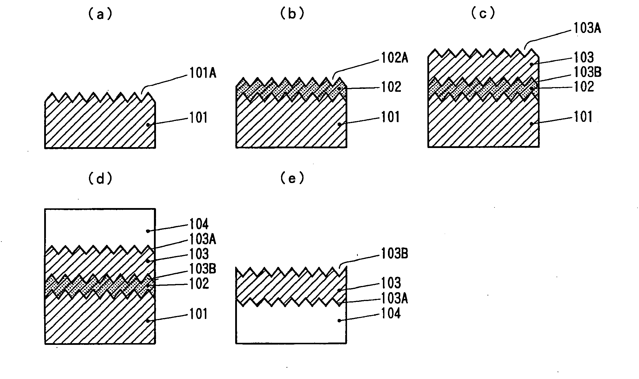
[0168](1) First, as shown in FIG. 10(a), a monocrystalline silicon substrate (such as 500 μm thick) 71 is prepared.

[0169]This monocrystalline silicon substrate 71 has a flat upper surface since a monocrystalline silicon sacrificial film, which will be described later, is to be epitaxially-grown.

[0170](2) Next, as shown in FIG. 10(b), on the monocrystalline silicon substrate 71, by a sputter-deposition method with substrate heating, silicon containing crystal defects is epitaxially-grown in an atmosphere containing small amounts of oxygen and water vapor. That is, a monocrystalline silicon sacrificial film (such as 0.1 to 1 μm thick) 72 containing crystal defects is formed. This monocrystalline silicon sacrificial film 72 can be easily and precisely removed by etching, as described later.

[0171](3) Next, as shown in FIG. 10(c), on the monocrystalline silicon sacrifi...

example 2

[0175]FIG. 12 includes cross-sectional views showing manufacturing steps of Example 2 according to the present invention.

[0176](1) First, as shown in FIG. 12(a), a monocrystalline silicon substrate (such as 500 μm thick) 81 is prepared.

[0177]This monocrystalline silicon substrate 81 has a flat upper surface since a monocrystalline silicon sacrificial film, which will be described later, is to be epitaxially-grown.

[0178](2) Next, as shown in FIG. 12(b), on the monocrystalline silicon substrate 81, by a sputter-deposition method with substrate heating, silicon containing crystal defects is epitaxially-grown in an atmosphere containing small amounts of oxygen and water vapor. That is, a monocrystalline silicon sacrificial film (such as 0.1 to 1 μm thick) 82 is formed. This monocrystalline silicon sacrificial film 82 can be easily and precisely removed by etching, as described later.

[0179](3) Next, as shown in FIG. 12(c), on the monocrystalline silicon sacrificial film 82, monocrystalli...

example 3

[0183]FIG. 13 includes cross-sectional views showing manufacturing steps of a monocrystalline thin film of Example 3 according to the present invention.

[0184]This example is the same as Examples 1 and 2 except that holes 91A are formed in a monodrystalline silicon substrate 91 at intervals. That is,

[0185](1) first, as shown in FIG. 13(a), the monocrystalline silicon substrate 91 is prepared in which the holes 91A are provided at intervals.

[0186]An optical microscope photograph of a plane surface of the monocrystalline silicon substrate 91 is shown FIG. 14 in which the holes 91A of 100 μm in diameter are formed at 1 mm intervals by photolithography and selective etching.

[0187](2) Next, as shown in FIG. 13(b), on the monocrystalline silicon substrate 91, by a sputter-deposition method with substrate heating, silicon containing defects is epitaxially-grown in an atmosphere containing small amounts of oxygen and water vapor. That is, a monocrystalline silicon sacrificial film 92 is form...


PUM

PropertyMeasurementUnit
Temperatureaaaaaaaaaa
Thicknessaaaaaaaaaa

Abstract

The present invention provides a method for manufacturing a monocrystalline film and a device formed by the above method, and according to the method mentioned above, lift-off of the monocrystalline silicon film is preferably performed and a high-purity monocrystalline silicon film can be obtained. A monocrystalline silicon substrate (template Si substrate) 201 is prepared, and on this monocrystalline silicon substrate 201, an epitaxial sacrificial layer 202 is formed. Subsequently, on this sacrificial layer 202, a monocrystalline silicon thin film 203 is rapidly epitaxially-grown using a RVD method, followed by etching of the sacrificial layer 202, whereby a monocrystalline silicon thin film 204 used as a photovoltaic layer of solar cells is formed.

Description

TECHNICAL FIELD[0001]The present invention relates to a method for manufacturing a monocrystalline thin film and a monocrystalline thin film device manufactured using the above method, and more particularly, relates to a method for manufacturing a high-purity monocrystalline silicon thin film for solar cells and a solar cell containing the monocrystalline silicon thin film manufactured by the above method.BACKGROUND ART[0002]Hereinafter, conventional methods for manufacturing a monocrystalline silicon thin film will be described.[0003](a) Oxygen Ion Implantation Method[0004]Oxygen ions are implanted into a monocrystalline silicon substrate, followed by heat treatment, so that a layered structure is formed which is composed of monocrystalline silicon, silicon dioxide, and the monocrystalline silicon substrate.[0005]However, when oxygen ions are implanted into the monocrystalline silicon substrate, problems may arise in that many defects are generated in upper-side monocrystalline sil...

Claims


Application Information

Patent Timeline
IPC IPC(8): H01L31/00H01L21/00C23C16/01C30B25/02C30B29/06C30B33/00H01L21/20H01L21/205H01L31/0392H01L31/04H01L31/18
CPCC30B25/02C30B29/06C30B33/00H01L21/02381H01L21/0245Y02E10/547H01L21/02634H01L21/02664H01L31/03921H01L31/1804H01L21/02532Y02P70/50
Inventor NODA, SUGURU
Owner JAPAN SCI & TECH CORP
Why Eureka
Try Eureka