Enhancement mode insulated gate heterostructure field-effect transistor

a heterostructure field-effect transistor and enhancement mode technology, applied in the direction of basic electric elements, electrical appliances, semiconductor devices, etc., can solve the problems of consuming power of depletion mode devices, and reducing the overall system power efficiency, so as to achieve precise threshold voltage control, enhance the operation mode, and reduce the effect of power consumption

Active Publication Date: 2008-08-28
SENSOR ELECTRONICS TECH
View PDF16 Cites 105 Cited by
  • Summary
  • Abstract
  • Description
  • Claims
  • Application Information

AI Technical Summary

Benefits of technology

[0010]Aspects of the present invention are directed to a semiconductor device based on the strain—energy-band engineering technique, double heterostructure design, MOSHFET technology, and quaternary alloy technology, which allows for enhancement mode o

Problems solved by technology

Depletion mode devices have several significant drawbacks for practical applications.
For example, depletion mode devices consume power when no gate voltage (i.e., input signal) is applied.
This decreases the overall system power efficiency, which has a negative impact on integrated digital electronics and power electronic circuits utilizing HFETs.
However, such a “normally-off” performance is hardly achievable in a regular GaN-based HFET design due to the presence of 2D electron

Method used


Image

  • Enhancement mode insulated gate heterostructure field-effect transistor
  • Enhancement mode insulated gate heterostructure field-effect transistor
  • Enhancement mode insulated gate heterostructure field-effect transistor

Examples


Embodiment Construction

[0023]It is understood that for the purposes of the disclosure, Al means Aluminum, As means Arsenic, Ga means Gallium, Hf means Hafnium, In means Indium, O means Oxygen, N means Nitrogen, and Si means Silicon. Further, it is understood that the phrase “any solution” means any now known or later developed solution.

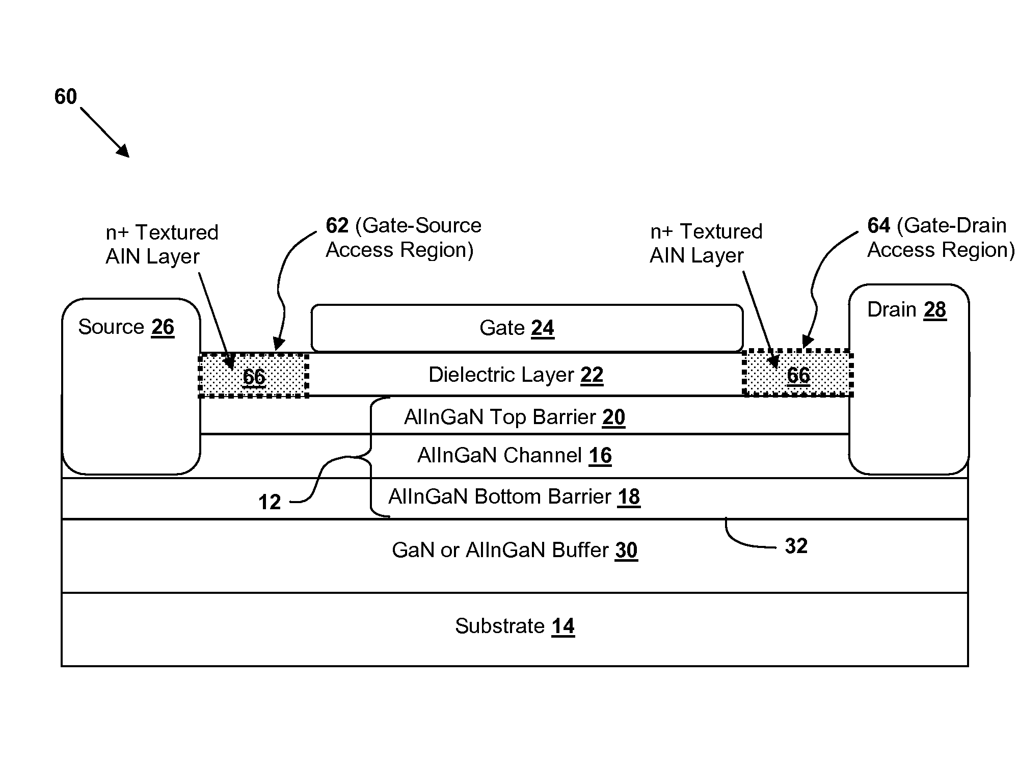
[0024]As detailed above, aspects of the present invention provide an enhancement mode (E-mode) insulated gate (IG) double heterostructure field-effect transistor (DHFET) having low power consumption at zero gate bias, low gate currents, and / or high reliability. Circuit design can be simplified by eliminating the need for bipolar voltage sources.

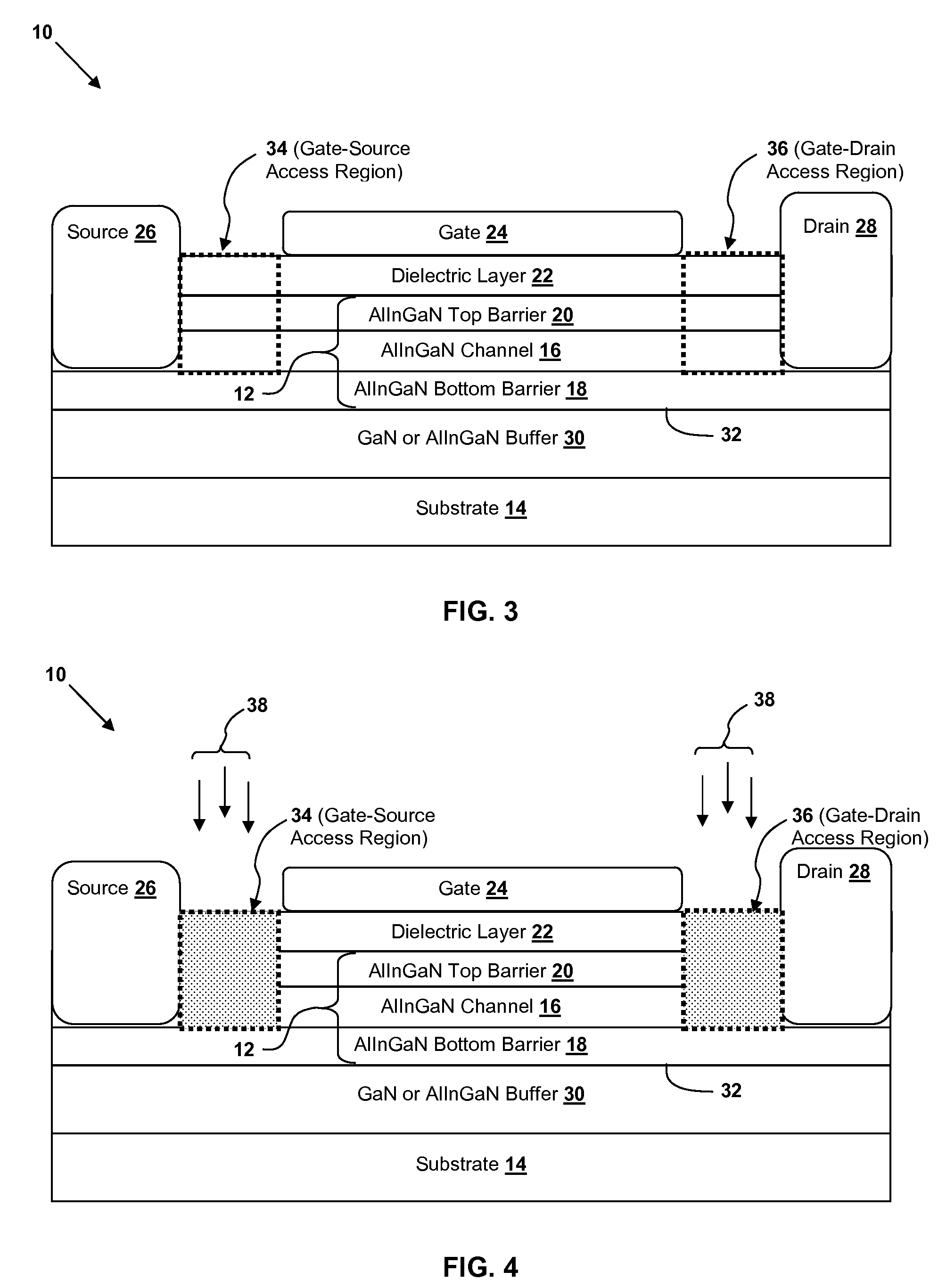
[0025]The epitaxial structure of an illustrative E-mode IG-DHFET 10 in accordance with an embodiment is depicted in FIG. 3. The IG-DHFET 10 comprises an AlInGaN / AlInGaN / AlInGaN heterostructure 12 grown over an insulating substrate 14. The insulating substrate 14 can be formed of any suitable material including, for example, sapphire,...


PUM


Abstract

Aspects of the present invention provide an enhancement mode (E-mode) insulated gate (IG) double heterostructure field-effect transistor (DHFET) having low power consumption at zero gate bias, low gate currents, and/or high reliability. An E-mode HFET in accordance with an embodiment of the invention includes: top and bottom barrier layers; and a channel layer sandwiched between the bottom and the top barrier layers, wherein the bottom and top barrier layers have a larger bandgap than the channel layer, and wherein polarization charges of the bottom barrier layer deplete the channel layer and polarization charges of the top barrier layer induce carriers in the channel layer; and wherein a total polarization charge in the bottom barrier layer is larger than a total polarization charge in the top barrier layer such that the channel layer is substantially depleted at zero gate bias.

Description

REFERENCE TO PRIOR APPLICATION[0001]The current application claims priority to co-pending U.S. Provisional Application No. 60 / 927,983, entitled “Enhancement Mode Insulated Gate Heterostructure Field-Effect Transistor,” filed on May 7, 2007, and hereby incorporated herein by reference.[0002]Aspects of the current application are also related to co-pending U.S. Provisional Application No. 60 / 903,104, entitled “Radio-Frequency Enhanced Contacts to Semiconductor Devices”, filed on Feb. 23, 2007, co-pending U.S. Provisional Application No. 60 / 905,634, entitled “Radio-Frequency Enhanced Contacts to Semiconductor Devices”, filed on Mar. 8, 2007, co-pending U.S. Provisional Application No. 60 / 903,109, entitled “Method of fabrication of radio-frequency enhanced contacts”, filed on Feb. 23, 2007, U.S. Provisional Application No. 60 / 905,725, entitled “Method of fabrication of semiconductor devices with radio-frequency enhanced contacts”, filed on Mar. 8, 2007, co-pending U.S. Utility applicati...

Claims


Application Information

Patent Timeline
IPC IPC(8): H01L29/778
CPCH01L29/2003H01L29/7783H01L29/402
Inventor SIMIN, GRIGORYSHUR, MICHAELGASKA, REMIGIJUS
Owner SENSOR ELECTRONICS TECH
Why Eureka
Try Eureka