Manufacturing method for a nanocrystal based device covered with a layer of nitride deposited by CVD

a nanocrystal and nitride technology, applied in the direction of nanotechnology, nanotechnology, coatings, etc., can solve the problems of increasing the capacity of flash memories and their miniaturisation, reducing the thickness of tunnel oxide, reducing the operating voltage, and increasing the leakage current through

Inactive Publication Date: 2008-08-28
COMMISSARIAT A LENERGIE ATOMIQUE ET AUX ENERGIES ALTERNATIVES
View PDF4 Cites 5 Cited by
  • Summary
  • Abstract
  • Description
  • Claims
  • Application Information

AI Technical Summary

Problems solved by technology

However, several technological obstacles start to bar the continuation of the increase in the capacities of the flash memories and their miniaturisation.
Unfortunately, the reduction in the thickness of the tunnel oxide, in particular below 8 nm, gives rise to an increase in the leakage currents through it due to the direct tunnel effect or by defects in this oxide, caused by the repetition of writing and erasing stresses (phenomenon called SILC: “Strain Induced Leakage Current”).
Another major problem is the reduction of the operating voltages to reduce the energy consumption and to be closer to the low operating voltages (1 to 2 Volts) of the CMOS (Complementary MOS) logic transistors.
Consequently, the presence of a defect in the tunnel oxide, which causes complete discharge in the case of a continuous floating gate device, will only affect the load situated upstream of the defect.
However, nanocrystal memories also have their limits.
In particular, these memories have low capacitive coupling between the control gate and the floating gate, which therefore requires the programming voltages to be maintained at a high level and which partially reduces the advantages related to the reduction of the tunnel oxide.
Another limit is that the threshold voltage offsets obtained with these devices are quite low, mainly due to the low cover rate of the active surface by the silicon nanocrystals (between 5×10¹¹ and 1012 per cm2 with a LPCVD (“Low Pressure Chemical Vapour Deposition”) deposition method that is widely used at present for these memories).
Another disadvantage is the dispersion of the size and the position of the nanocrystals on the tunnel oxide, which causes a dispersion of the memory characteristics.
Another major difficulty posed by nanocrystal devices lies in their integration with the other manufacturing steps of flash type memories.
The problem here is that of the oxidation of the silicon nanocrystals during the subsequent steps, which are potentially oxidising, but also their oxidation with the ambient air.
The first problem posed by these two passivation techniques, NO annealing and plasma nitriding, is that they consume silicon nanocrystals during the formation of the passivation layer.
The second problem posed by these two passivation techniques relates to the tunnel dielectric, or more specifically the tunnel oxide.
Indeed, during passivation, there is a risk of nitriding the tunnel oxide, which is not necessarily a problem, but care must however be taken to avoid downgrading the electrical properties of this tunnel oxide.
A third problem is the formation of a native oxide at the surface of the nanocrystals.
However, according to document [1], nanocrystals of this dimension do not permit in practice cover rates to be obtained that are sufficient to obtain a satisfactory threshold voltage offset with low dispersion.
This is a positive point for the passivation of the nanocrystals, but poses a real problem for the tunnel oxide.
Indeed, it is thought that Nitrogen plasma treatment is detrimental to the reliability of the tunnel oxide.
Furthermore, the operating conditions required for the plasma nitriding (which is to say 20 minutes at 800° C. for single plate equipment) are not conditions easily used in an “industrial” orientated method.

Method used


Image

  • Manufacturing method for a nanocrystal based device covered with a layer of nitride deposited by CVD
  • Manufacturing method for a nanocrystal based device covered with a layer of nitride deposited by CVD

Examples


Embodiment Construction

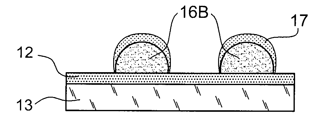
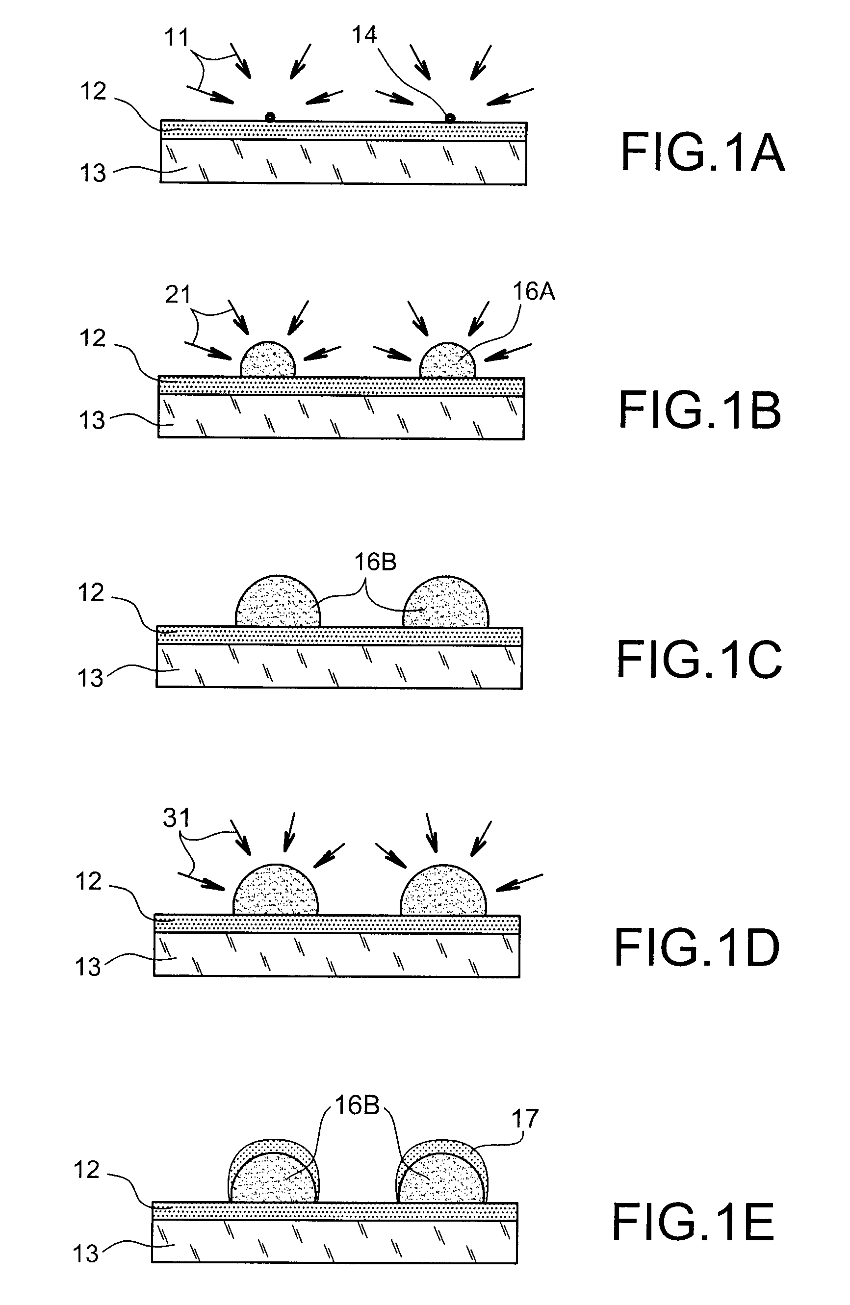
[0034]This purpose is achieved by a CVD (“Chemical Vapour Deposition”) method comprising both the creation of the nanocrystals of determined size and density and their passivation, in the form of stoichiometric nitride deposition only located on the nanocrystals. It is therefore possible to make silicon nanocrystals covered with a layer of silicon nitride.

[0035]The method according to the invention is a manufacturing method for a structure comprising semi-conductor material nanocrystals on a dielectric material substrate by chemical vapour deposition (CVD), the nanocrystals being covered by a layer of semi-conductor material nitride, said method comprising:[0036]a germination step by the formation on the dielectric material substrate of stable nuclei in the form of islands, by CVD from a first gaseous precursor of the nuclei selected so that the dielectric material accepts the formation of said nuclei,[0037]a growth step by the formation of semi-conductor material nanocrystals from ...


PUM

PropertyMeasurementUnit
sizeaaaaaaaaaa
thicknessaaaaaaaaaa
thicknessaaaaaaaaaa

Abstract

The invention relates to a manufacturing method for a structure comprising semi-conductor material nanocrystals on a dielectric material substrate by chemical vapour deposition (CVD), the nanocrystals being covered by a layer of semi-conductor material nitride. The method comprises a step for forming stable nuclei on the substrate by CVD from a first gaseous precursor of the nuclei; a step of nanocrystal growth from stable nuclei by CVD from a second gaseous precursor; and a step for forming a layer of semi-conductor material nitride on the nanocrystals. The method is characterised in that the passivation step is carried out by selective and stoichiometric CVD of semi-conductor material nitride only on the nanocrystals from a mixture of the second and a third gaseous precursor selected to cause selective and stoichiometric deposition of the nitride only on said nanocrystals, wherein steps for forming the nuclei, forming the nanocrystals and passivation are carried out inside a same, single chamber.
The invention also relates to the formation of memory cells and flash memories comprising nanocrystals made according to the method of the invention.

Description

TECHNICAL FIELD[0001]The invention relates to a manufacturing method for a device comprising nanocrystals, of determined size and density, covered with a layer of nitride deposited by CVD. The method permits, in particular, memory cells to be obtained to make flash memories.STATE OF THE PRIOR ART[0002]Flash memories use field effect transistors as their base cells. These transistors feature a floating gate located between the channel and the control gate of the transistor, as well as a tunnel dielectric located between the channel of the transistor and the floating gate.[0003]The floating gate is the element which stores the information. In the current MOS (Metal Oxide Semiconductor) technology the floating gate is made of n-doped polycrystalline silicon.[0004]The tunnel dielectric is generally a thermal silicon oxide (SiO2). It is via this oxide that the loads are injected from the channel to the floating gate.[0005]In recent years, the capacities of flash memories have increased c...

Claims


Application Information

Patent Timeline
Patent Type & Authority Applications(United States)
IPC IPC(8): H01L29/788H01L21/20H01L21/285
CPCB82Y10/00C23C16/02H01L29/42332H01L21/28273C23C16/345H01L29/40114
Inventor COLONNA, JEAN-PHILIPPE
Owner COMMISSARIAT A LENERGIE ATOMIQUE ET AUX ENERGIES ALTERNATIVES
Why Eureka
Try Eureka