

Semiconductor integrated circuit device and fabrication method for the same
- Summary
- Abstract
- Description
- Claims
- Application Information
AI Technical Summary
Benefits of technology
Problems solved by technology
Method used
Image

Examples
embodiment 1
[0094]A semiconductor integrated circuit device and a fabrication method for the same of Embodiment 1 of the present invention will be described with reference to the relevant drawings.
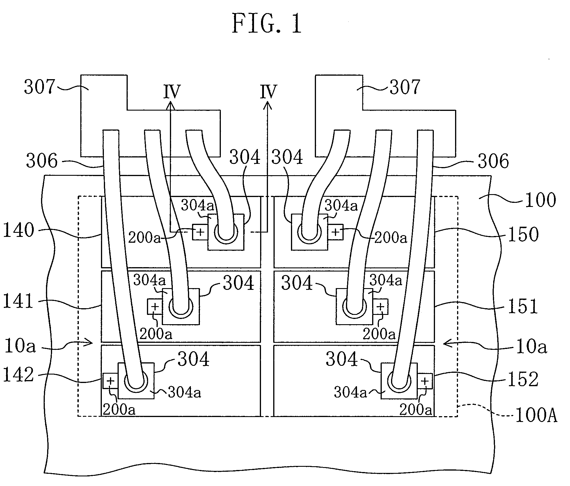
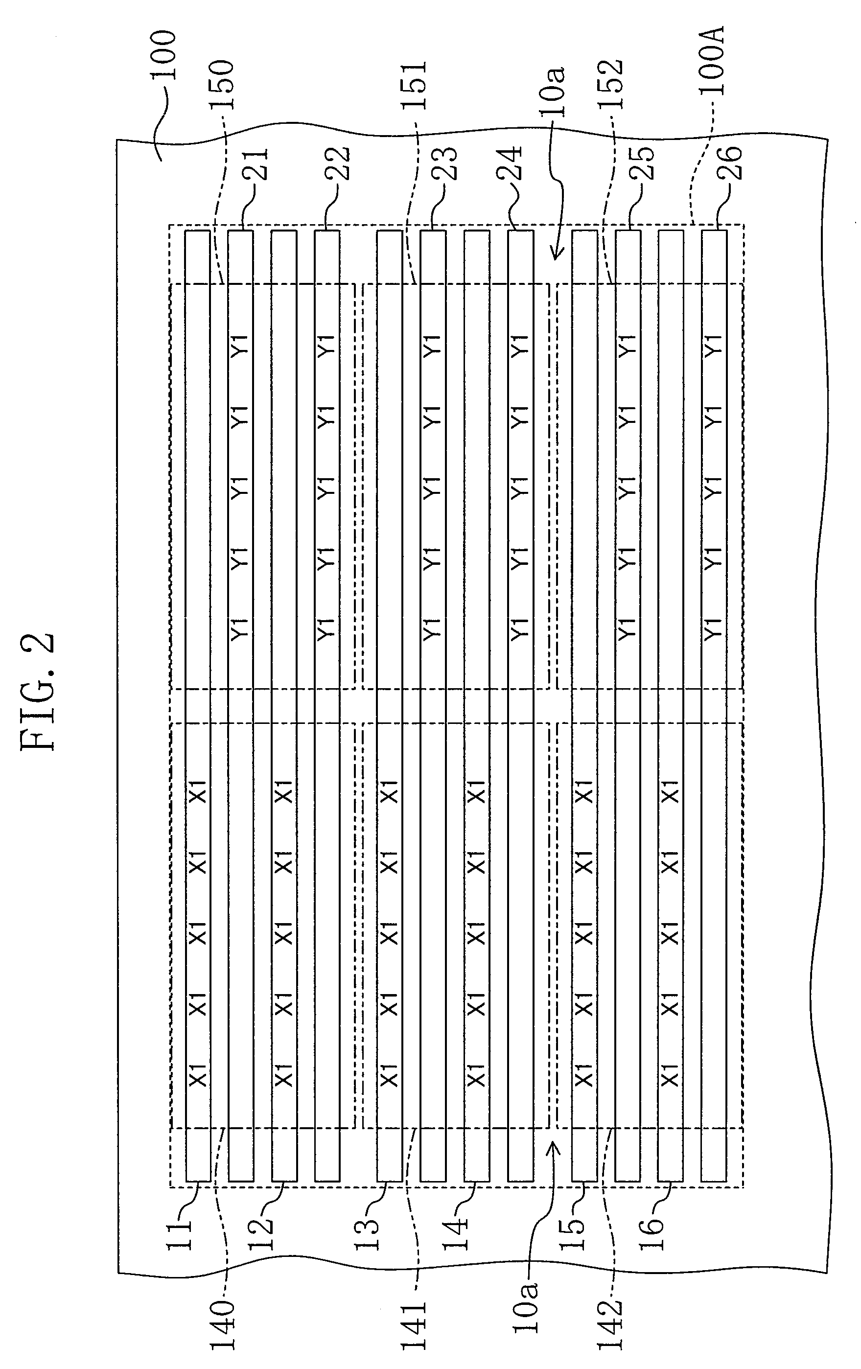
[0095]FIG. 1 is a simplified plan view of part of the semiconductor integrated circuit device of Embodiment 1 of the present invention.
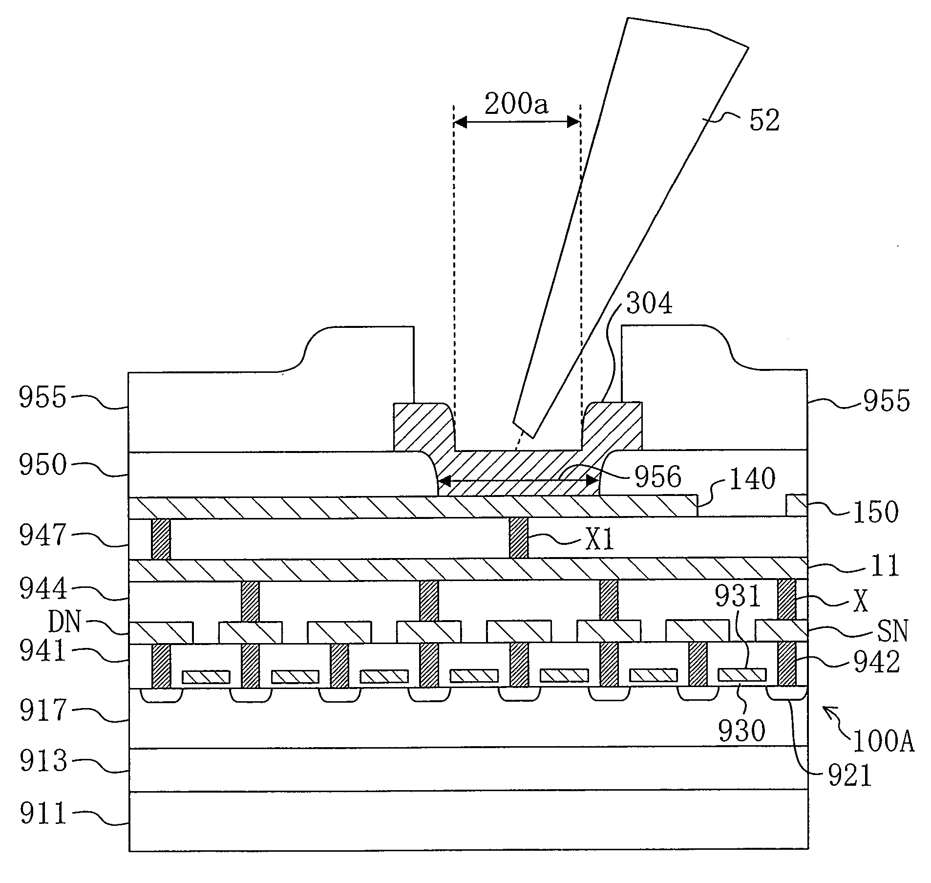
[0096]As shown in the plan view of FIG. 1, a power transistor 100A surrounded with an isolation layer is formed as an active element in an IC chip 100. Buses 140 to 142 and buses 150 to 152 are formed to cover source and drain regions of the power transistor 100A. The buses 140 to 142, which are in a topmost metal layer (third metal layer) made of sheet-like metal, are connected with source electrodes. The buses 140 to 142 are obtained by dividing a large-size bus equally with slits 10a. Likewise, the buses 150 to 152, which are in the topmost metal layer (third metal layer) made of sheet-like metal, are connected with drain electrodes. The buses 150 to 152 are obtaine...
embodiment 2
[0116]A semiconductor integrated circuit device and a fabrication method for the same of Embodiment 2 of the present invention will be described with reference to the relevant drawings.
[0117]FIG. 7 is a simplified plan view of part of the semiconductor integrated circuit device of Embodiment 2 of the present invention.
[0118]As shown in the plan view of FIG. 7, a power transistor 100A surrounded with an isolation layer is formed as an active element in an IC chip 100. Buses 140 to 142 and buses 150 to 152 are formed to cover source and drain regions of the power transistor 100A. The buses 140 to 142, which are in a topmost metal layer (third metal layer) made of sheet-like metal, are connected with source electrodes. The buses 140 to 142 are obtained by dividing a large-size bus equally with slits 10a. Likewise, the buses 150 to 152, which are in the topmost metal layer (third metal layer) made of sheet-like metal, are connected with drain electrodes. The buses 150 to 152 are obtaine...
embodiment 3
[0121]Semiconductor integrated circuits and fabrication methods for the same of Embodiment 3 of the present invention will be described with reference to the relevant drawings.
[0122]FIGS. 8A and 8B are simplified plan views of part of semiconductor integrated circuits of Embodiment 3 of the present invention.
[0123]As shown in the plan view of FIG. 8A, a power transistor 100A surrounded with an isolation layer is formed in an IC chip 100. A single first bus 140 and a single second bus 150 are formed to cover source and drain regions of the power transistor 100A. The first bus 140, which is in a topmost metal layer (third metal layer) made of sheet-like metal, is connected to source electrodes. Likewise, the second bus 150, which is also in the topmost metal layer (third metal layer) made of sheet-like metal, is connected to drain electrodes. One contact pad 304 is formed on each of the first and second buses 140 and 150. The contact pad 304 has a bonding region 304a and a probe testi...
PUM
 Abstract
Description
Claims
Application Information