Methods for fabricating complex micro and nanoscale structures and electronic devices and components made by the same

a technology of electronic devices and components, applied in photomechanical devices, instruments, nuclear engineering, etc., can solve the problems of increasing net processing costs at an exponential rate, impede the full integration of this technology, and use of multiple resists and multiple developers is very costly and laborious

Active Publication Date: 2008-10-16
THE BOARD OF TRUSTEES OF THE UNIV OF ILLINOIS
View PDF51 Cites 29 Cited by
  • Summary
  • Abstract
  • Description
  • Claims
  • Application Information

AI Technical Summary

Benefits of technology

[0033]In another aspect, the present invention provides an electronic device made by a method comprising the steps of: (i) providing a layer of photosensitive material on at least a portion of a substrate; (ii) exposing a first area of said layer of photosensitive material to radiation having a first intensity; (iii) exposing a second area of said layer of photosensitive material to radiation having a second intensity; wherein said second area of said layer partially overlaps said first area of said layer; (iv) developing said layer of photosensitive material by removing material from said first and second areas, thereby generating a recessed feature in said layer having a non-uniform depth profile, wherein said recessed feature exposes an exposed region of sa...

Problems solved by technology

Processing methods for making T-gates and G-gates using multiple resist stacks have several important disadvantages that impede full integration of this technology.
First, use of multiple resists and multiple developers is very costly and labor intensive.
This is largely because several separate resist deposition and development processing steps are involved, which increase net processing costs at an exponential rate.
Second, use of multiple resist layers during processing inevitably results in intermixing of the applied resist layers, which can result in significant deviations in the cross-sectional geometry of the gate structure achieved.
Third, the baking temperature required for a second resist laye...

Method used


Image

  • Methods for fabricating complex micro and nanoscale structures and electronic devices and components made by the same
  • Methods for fabricating complex micro and nanoscale structures and electronic devices and components made by the same
  • Methods for fabricating complex micro and nanoscale structures and electronic devices and components made by the same

Examples


example 1

Fabrication of a T-Gate Structure for a HEMT Device

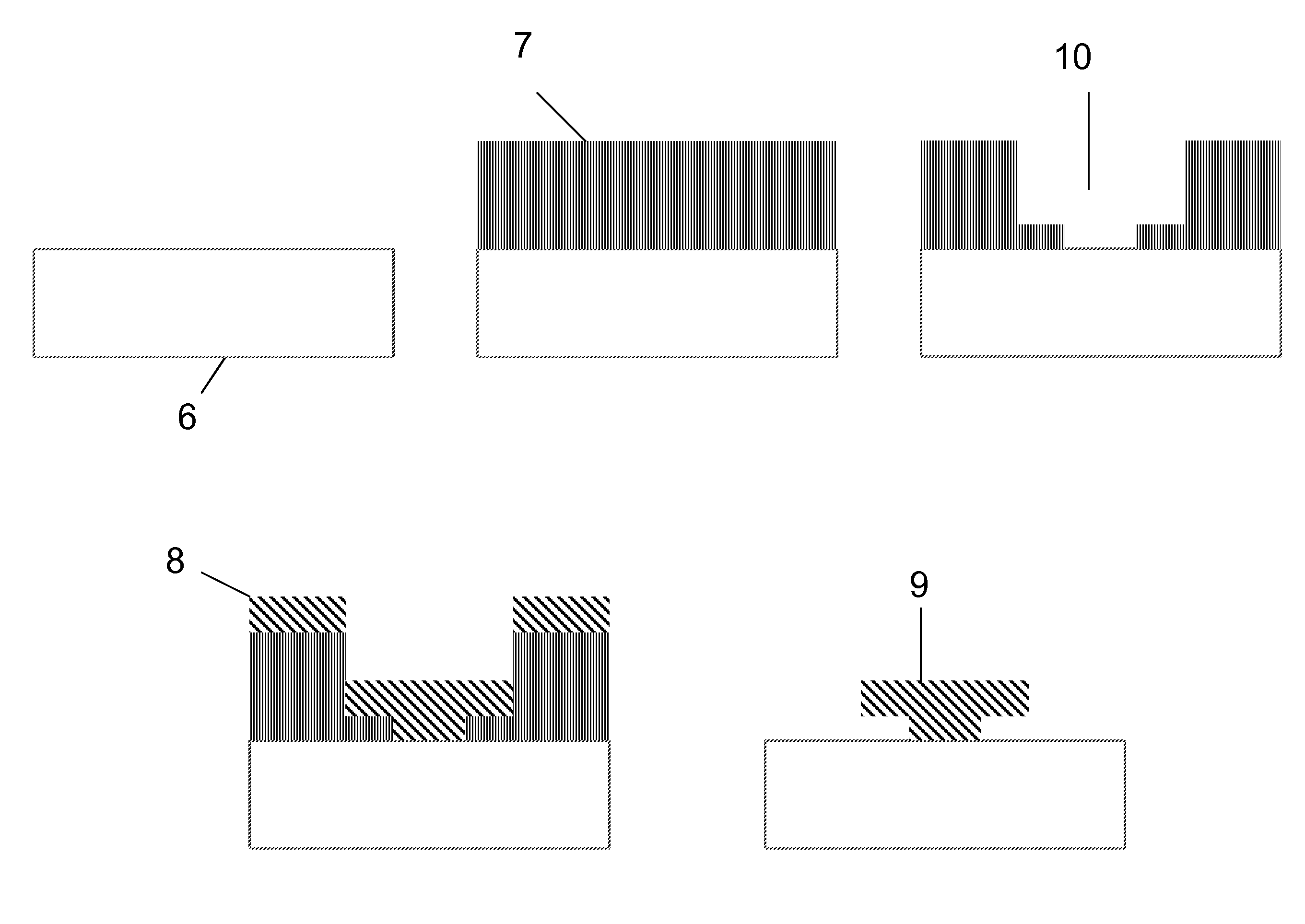
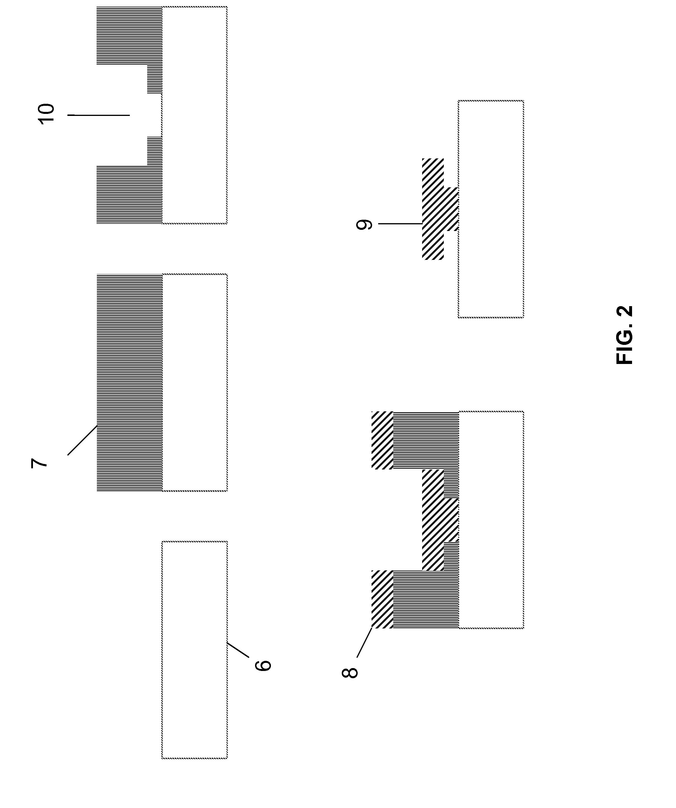
[0074]This example demonstrates the patterning a T-Gate structure which acts as the Schottky contact for a GaN / AlGaN HEMT structure using the methods of the present invention. The patterning of the gate is one of the most important steps for device performance and is usually patterned at the very end after the rest of the processing has been completed.

[0075]A 7000 Å layer of PMMA is spun on the substrate using certain spin speed and spin time. The substrate having the PMMA layer is exposed to an electron beam, which first writes a rectangle having a length of 150 nm at a dose of 50%. Another rectangle having a length of 150 nm is subsequently written such that it partially overlaps the first rectangle. The second rectangle is written with a 50% dose and covers half the area of the first rectangle. The sample is developed in MIBK: IPA (1:3). The exposed regions dissolve in the developer. About 250 Å of Nickel and 3000 Å of Gold are d...


PUM


Abstract

This invention provides processing steps, methods and materials strategies for making patterns of structures for electronic, optical and optoelectronic devices. Processing methods of the present invention are capable of making micro- and nano-scale electronic structures, such as T-gates, gamma gates, and shifted T-gates, having a selected non-uniform cross-sectional geometry. The present invention provides lithographic processing strategies for sub-pixel patterning in a single layer of photoresist useful for making and integrating device components comprising dielectric, conducting, metal or semiconductor structures having non-uniform cross-sectional geometries. Processing methods of the present invention are complementary to conventional microfabrication and nanofabrication platforms, and can be effectively integrated into existing photolithographic, etching and thin film deposition patterning strategies, systems and infrastructure.

Description

CROSS-REFERENCE TO RELATED APPLICATIONS[0001]Not applicableSTATEMENT REGARDING FEDERALLY SPONSORED RESEARCH OR DEVELOPMENT[0002]Not ApplicableBACKGROUND OF INVENTION[0003]Advanced microfabrication and nanofabrication patterning techniques enable the fabrication and assembly of structures on substrate surfaces. The spectrum of available patterning techniques includes photolithography, soft lithography (e.g., contact printing), electron beam direct writing, and photoablation patterning methods. This suite of available patterning techniques is compatible with a wide range of substrates and deposition materials, including high quality semiconductors, dielectrics and conducting materials, and is compatible with processing a useful range of substrate materials, morphologies, and sizes. In combination with state of the art resist processing and materials deposition techniques, advanced patterning techniques provide a high degree of deterministic control over the physical dimensions and spa...

Claims


Application Information

Patent Timeline
IPC IPC(8): H01L21/26H01L27/02
CPCB81B2203/0181H01L27/1288H01L21/0272B81C1/0015
Inventor JAIN, KANTIREDDY, UTTAM
Owner THE BOARD OF TRUSTEES OF THE UNIV OF ILLINOIS
Why Eureka
Try Eureka