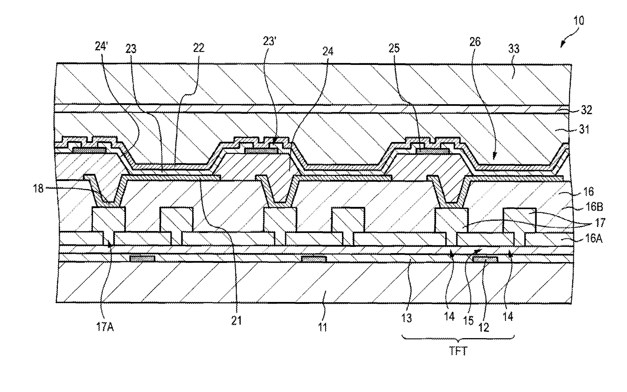
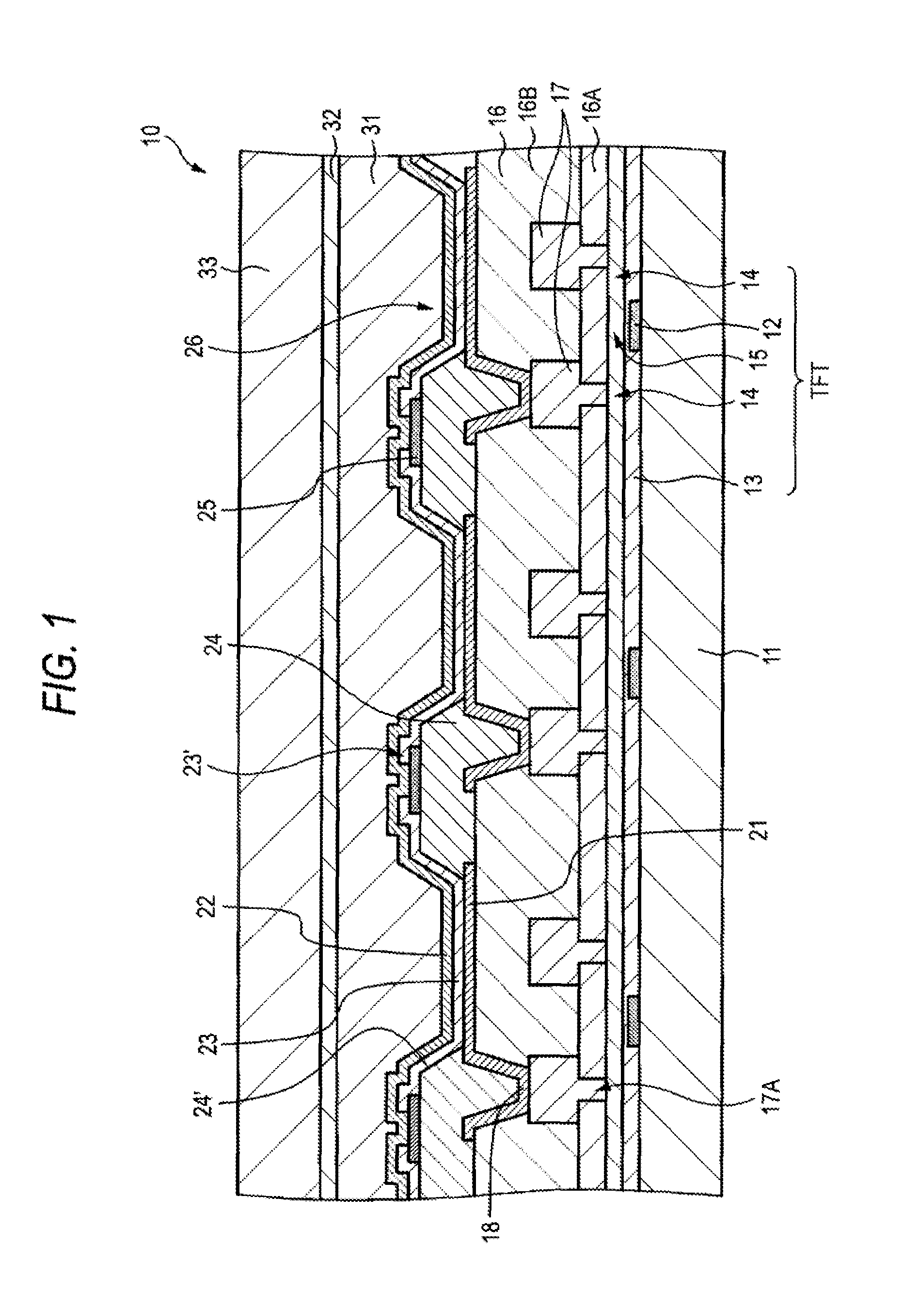
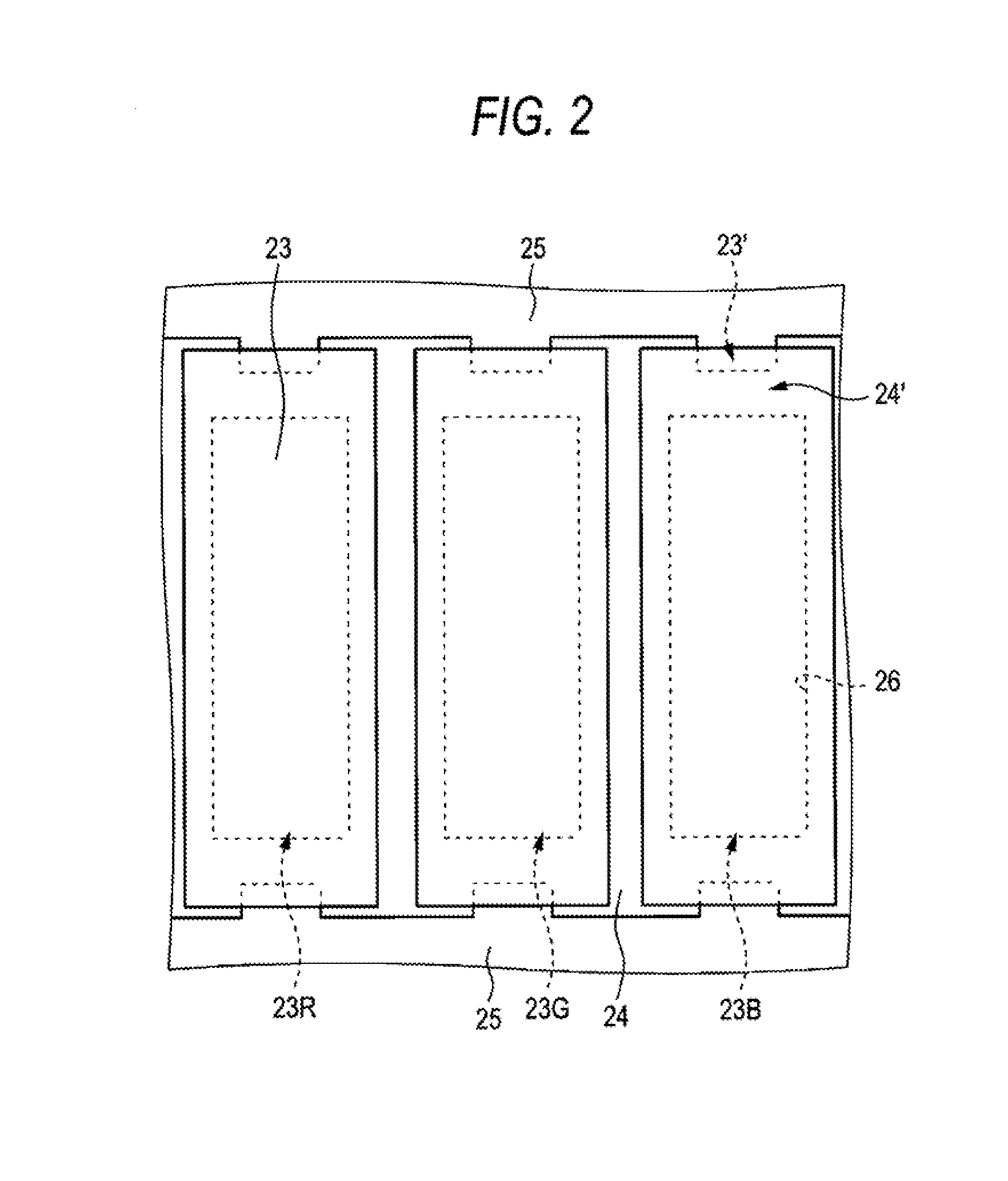
[0026]In the organic EL display device according to the second embodiment, the two-layer structure layer extends between the upper electrode and the insulating layer and further, the two-layer structure layer extends also between the stacked structure positioned over the lower electrode and the upper electrode. In case that the two-layer structure layer extends between the stacked structure and the upper electrode, specifically, the two-layer structure layer and the upper electrode formed thereon cover the stacked structures forming the plural organic electroluminescence elements. In this case, the two-layer structure layer and the upper electrode formed thereon can be formed by the same process, which can simplify the manufacturing process as well as reduces the number of masks to be used. In addition, in the organic EL display device according to the second embodiment, at least one layer of the stacked structure may include a portion touching the auxiliary wiring.
[0033]On the other hand, when the organic EL display device is the top-surface emitting type and the upper electrode is used as the
cathode electrode, it is preferable that the upper electrode is made of a conductive material whose value of the
work function is small so as to allow emitted light to be transmitted therethrough as well as to allow electrons to be efficiently injected with respect to the stacked structure. Specifically, it is preferable to use a conductive film as the upper electrode, which has high light
transmittance such as a Mg—
Ag alloy thin film (for example, a
metal or an
alloy material whose light
transmittance is 30% or more) as described above. Note that the upper electrode is liable not to function as an electrode if the thickness of the upper electrode made of the Mg—Au
alloy is not more than 4 nm. If the thickness exceeds 20 nm, the electrode is liable not to be suitable for the upper electrode because the light
transmittance is reduced. When the upper electrode is used as the
anode electrode, it is preferable that the upper electrode is made of a conductive material through which emitted light is transmitted and whose value of the
work function is large. The upper electrode is preferably formed by a
deposition process which is a process in which energy of deposition particles is small such as the
vacuum deposition process or a MOCVD process from a viewpoint that damages in the stacked structure is prevented from occurring. If damages occur in the stacked structure, a non-emitting pixel (or non-emitting sub pixel) which is called as a “
dark spot” is liable to be generated due to occurrence of leak current. In addition, it is preferable that the formation of the stacked structure to the formation of the upper electrode is executed without being exposed to air from a viewpoint of preventing deterioration of the stacked structure due to
moisture in air. When the upper electrode is used as a
cathode electrode, an
electron injection layer having the same pattern as the upper electrode (for example, made of Lif which is extremely thin, the thickness of which is 0.3 nm) may be formed just under the upper electrode, thereby increasing the
electron injection ability, realizing low drive
voltage, high efficiency and long life of the organic EL elements.
[0034]In an embodiment, it is preferable that the insulating layer is made of an insulating material having excellent flatness and low water-absorbing property for preventing deterioration of the stacked structure due to
moisture to keep light-emitting luminance, specifically, organic insulating materials such as
polyimide resin,
photoresist materials and the like can be cited.
[0040]It is preferable that an insulating or conductive protection film is provided on the upper electrode for preventing
moisture from reaching the stacked structure. The protection film is preferably formed based on a
deposition process in which energy of deposition particles is small particularly such as a
vacuum deposition process, or formed by a MOCVD process, which can reduce effects on the base. It is also preferable that the protection film is deposited by setting
deposition temperature to be constant for preventing reduction of luminance due to deterioration of the stacked structure, and further, it is preferably deposited under conditions minimizing the stress on the protection film for preventing the peeling of the protection film. In addition, it is preferable that the protection film is formed without exposing the upper electrode to air, which prevents deterioration of the stacked structure due to moisture or
oxygen in air. In case that the organic EL display device is the top-surface emitting type, the protection film is preferably made of a material through which, for example, more than 80% of light generated in the stacked structure is transmitted, specifically, inorganic-amorphous insulating materials such as
amorphous silicon (α-Si),
amorphous silicon carbide (α-SiC),
amorphous silicon nitride (α-Si1-X-Nx), amorphous
silicon oxide (α-Si1-yOy),
amorphous carbon (α-C) can be cited. Since such inorganic-amorphous insulating materials do not generate grains, water permeability is low and can form the good protection film. When the protection film is made of a conductive material, the protection film may be made of a transparent conductive material such as ITO or IZO. The second substrate is arranged over the protection film, and the protection film and the second substrate are adhered by using a UV cure
adhesive or a heat cure
adhesive.
[0042]In the organic EL display device according to the first embodiment, the stacked structure has a portion (overlapping portion) touching the auxiliary wiring, and the upper electrode covers the whole surface of the stacked structures and the auxiliary wiring forming plural organic EL elements. Therefore, it is certain that there does not exist the insulating layer just under a portion of the upper electrode connecting a portion of the upper electrode over the stacked structure to a portion of the upper electrode over the stacked structure. That is, the portion of the upper electrode connecting the portion of the upper electrode over the stacked structure to the portion of the upper electrode over the auxiliary wiring is formed at least on one layer of the plural
layers included in the stacked structure. In the organic EL display device according to the second embodiment, the upper electrode covers the stacked structures and the two-layer structure layer forming plural organic electroluminescence elements without touching the insulating layer. Therefore, a portion of the upper electrode connecting a portion of the upper electrode over the stacked structure and a portion of the upper electrode on the auxiliary wiring does not degenerate, thereby providing the organic EL display device having excellent display performance. In addition, in the organic EL display device according to the second embodiment, the upper electrode and the auxiliary wiring are electrically connected through the two-layer structure layer including a
charge injection layer and a charge
transport layer from below, therefore, charges (electrons or holes) are transported from the auxiliary wiring to the upper electrode through the
charge injection layer and the charge
transport layer without losing large voltage, as a result, voltage rising at an
electrical connection portion between the upper electrode and the auxiliary wiring can be suppressed as well as manufacturing processes can be simplified according to the state of the two-layer structure layer.

