Nitride substrates, thin films, heterostructures and devices for enhanced performance, and methods of making the same

a technology of nitride semiconductors and substrates, applied in the direction of crystal growth process, polycrystalline material growth, chemically reactive gases, etc., can solve the problems of nitride semiconductor devices that cannot meet achieve the theoretical performance potential, remain too fragile, and too expensive for high-power commercial and consumer use. , to achieve the effect of enhancing electrical efficiency, reducing the density of thread dislocations, and enhancing carrier mobility

Inactive Publication Date: 2008-12-04
INLUSTRA TECH
View PDF7 Cites 20 Cited by
  • Summary
  • Abstract
  • Description
  • Claims
  • Application Information

AI Technical Summary

Benefits of technology

[0025]The fifth class of products embodied by the present invention is fully integrated devices that incorporate substrates, templates, or heterostructures comprising a nitride semiconductor having a moderate density of basal plane stacking faults and a reduced density of threading dislocations. These devices would benefit from the enhanced carrier mobility provided in accordance with the present invention to enhance electrical efficiency, decrease heating, and generally improve performance. In general, the present invention can be broadly applied to a variety of electronic and optoelectronic devices based on the (Al,In,B,Ga)N materials system. For example, a light emitting diode (“LED”) can be produced that incorporates a substrate, template and/or heterostructure component comprising a nitride semiconductor having a moderate density of basal plane stacking faults and a reduced density

Problems solved by technology

Despite considerable progress, however, devices based on nitride semiconductors, including but not limited to laser diodes, light emitting diodes, photovoltaics, and power transistors (hereafter collectively referred to as “nitride devices”) have failed to attain their theoretical performance potential and have therefore remained too inefficient, too fragile, and too expensive for high-power commercial and consumer use.
Three of the major causes of this shortfall in device performance are polarization-related inefficiencies of conventional nitride devices, high defect de

Method used


Image

  • Nitride substrates, thin films, heterostructures and devices for enhanced performance, and methods of making the same
  • Nitride substrates, thin films, heterostructures and devices for enhanced performance, and methods of making the same
  • Nitride substrates, thin films, heterostructures and devices for enhanced performance, and methods of making the same

Examples


Embodiment Construction

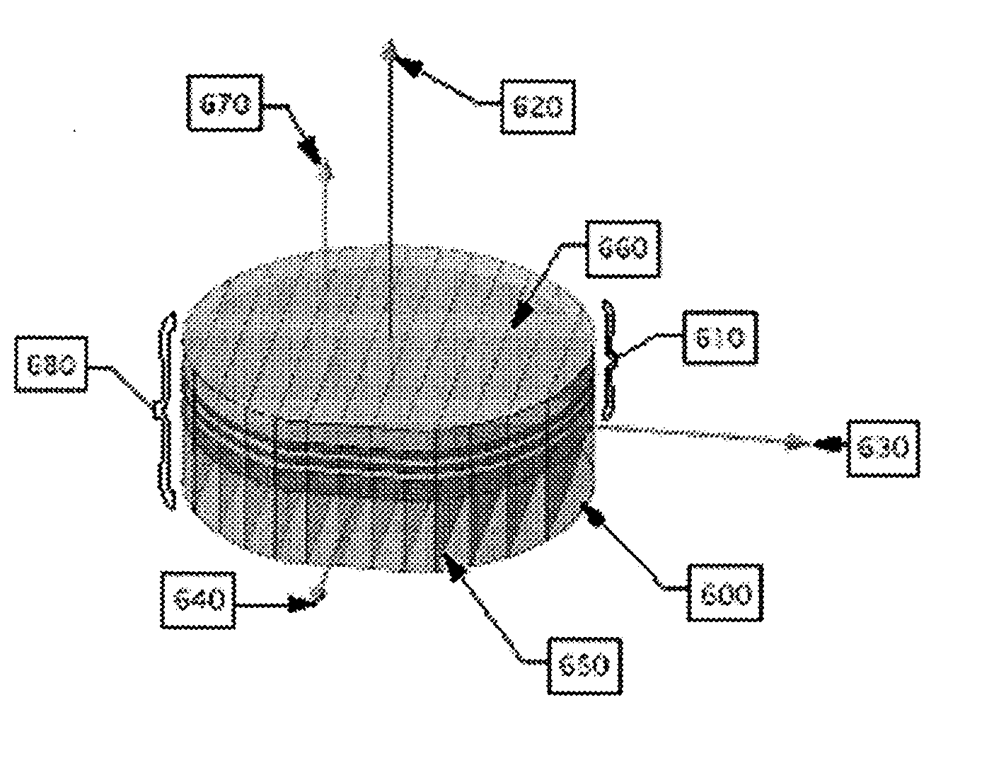
[0036]Referring now to FIG. 3, a substrate of the present invention comprising a nitride semiconductor having a moderate density of basal plane stacking faults and a reduced density of threading dislocations is shown. Block 300 represents a nitride semiconductor substrate comprising a crystalline matrix of (AlxByInzGa1−x−y−z)N, in which 0≦x≦1, 0≦y≦1, 0≦z≦1, and 0≦x+y+z≦1. This substrate can range in thickness from about 40 μm to about 2 mm in thickness. More preferably, the thickness can range from about 250 μm to about 2000 μm. In other embodiments, the substrate thickness can range from about 50 μm to about 500 μm in thickness. However, the substrates of the invention can be of any conceivable thickness, limited only by practical considerations that are dictated by the application for which the substrate will be used. Most commonly, substrates having thicknesses ranging from about 250 μm to about 500 μm are desirable for device layer re-growth in the nitride semiconductor device i...


PUM


Abstract

The present invention provides nitride semiconductors having a moderate density of basal plane stacking faults and a reduced density of threading dislocations, various products based on, incorporating or comprising the nitride semiconductors, including without limitation substrates, template films, templates, heterostructures with or without integrated substrates, and devices, and methods for fabrication of templates and substrates comprising the nitride semiconductors.

Description

REFERENCE TO RELATED APPLICATION[0001]This application is related to and claims the benefit of U.S. Provisional Application 60 / 940,922 filed May 30, 2007, the disclosure of which is incorporated herein by reference in its entirety.TECHNICAL FIELD[0002]The present invention relates to nitride semiconductors as well as substrates, thin films, templates, heterostructures and electronic devices based on, incorporating or comprising the nitride semiconductors and methods of making the same.BACKGROUND OF THE INVENTION[0003]Gallium nitride and its alloys with indium, aluminum, and boron nitride have attracted significant attention in recent years due to the successful development of visible and ultraviolet light emitting diodes (LEDs), blue / violet laser diodes, and high-power electronic devices based on this materials system. Revolutions in lighting, display technology, data storage, and power switching are occurring as a result of the unique optical, electronic, and structural properties ...

Claims


Application Information

Patent Timeline
IPC IPC(8): H01L29/205H01L21/205
CPCC30B25/02C30B29/403H01L21/0237H01L21/02458H01L21/0254H01L21/02573H01L21/02609H01L21/02639H01L21/02642H01L21/02647H01L29/045H01L29/2003H01L33/16H01L33/32
Inventor HASKELL, BENJAMINFINI, PAUL T.
Owner INLUSTRA TECH
Why Eureka
Try Eureka