Mount for a Semiconductor Light Emitting Device

a light-emitting device and semiconductor technology, applied in semiconductor devices, semiconductor/solid-state device details, electrical devices, etc., can solve the problems of inability to efficiently dissipate heat generated in the device by silicon mounts, and achieve the effect of efficient heat dissipation

Active Publication Date: 2008-12-11
PHILIPS LUMILEDS LIGHTING CO LLC
View PDF7 Cites 30 Cited by
  • Summary
  • Abstract
  • Description
  • Claims
  • Application Information

AI Technical Summary

Benefits of technology

[0006]In accordance with embodiments of the invention, a mount for a semiconductor device includes a carrier, at least two metal leads disposed on a bottom surface of the carrier, and a cavity extending through a thickness of the carrier to expose a portion of the top surfaces of the metal leads. A semiconductor light emitting device is positioned in the cavity and is electrically and physically connected to the metal leads. The carrier may be, for example, silicon, and the leads may be multilayer structures, for example a thin gold layer connected to a thick copper layer. Such an arrangement may efficiently conduct heat away from the semiconductor light emitting device, since the entire thermal path from the semiconductor structure through the leads is metal.

Problems solved by technology

As semiconductor light emitting devices are operated at higher power, silicon mounts become increasingly incapable of efficiently dissipating the heat generated in the device.

Method used


Image

  • Mount for a Semiconductor Light Emitting Device
  • Mount for a Semiconductor Light Emitting Device
  • Mount for a Semiconductor Light Emitting Device

Examples


Embodiment Construction

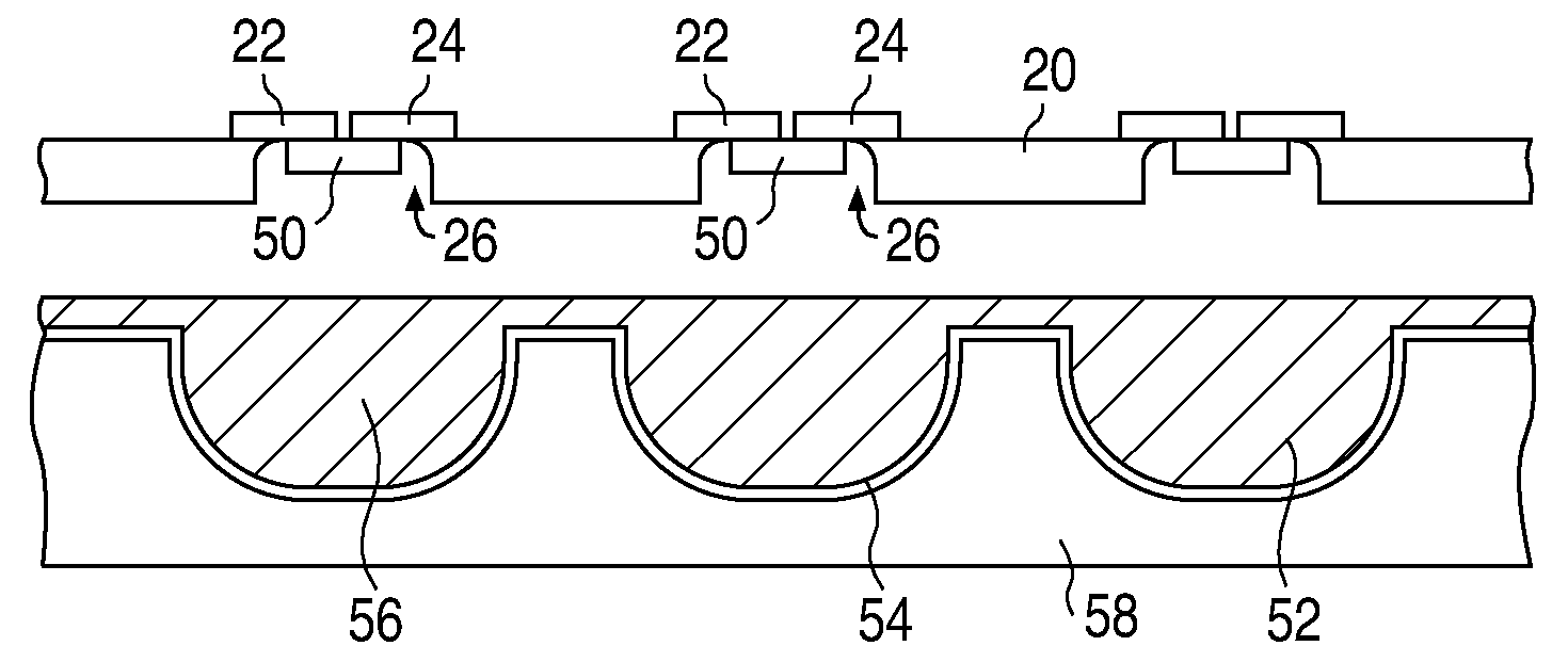
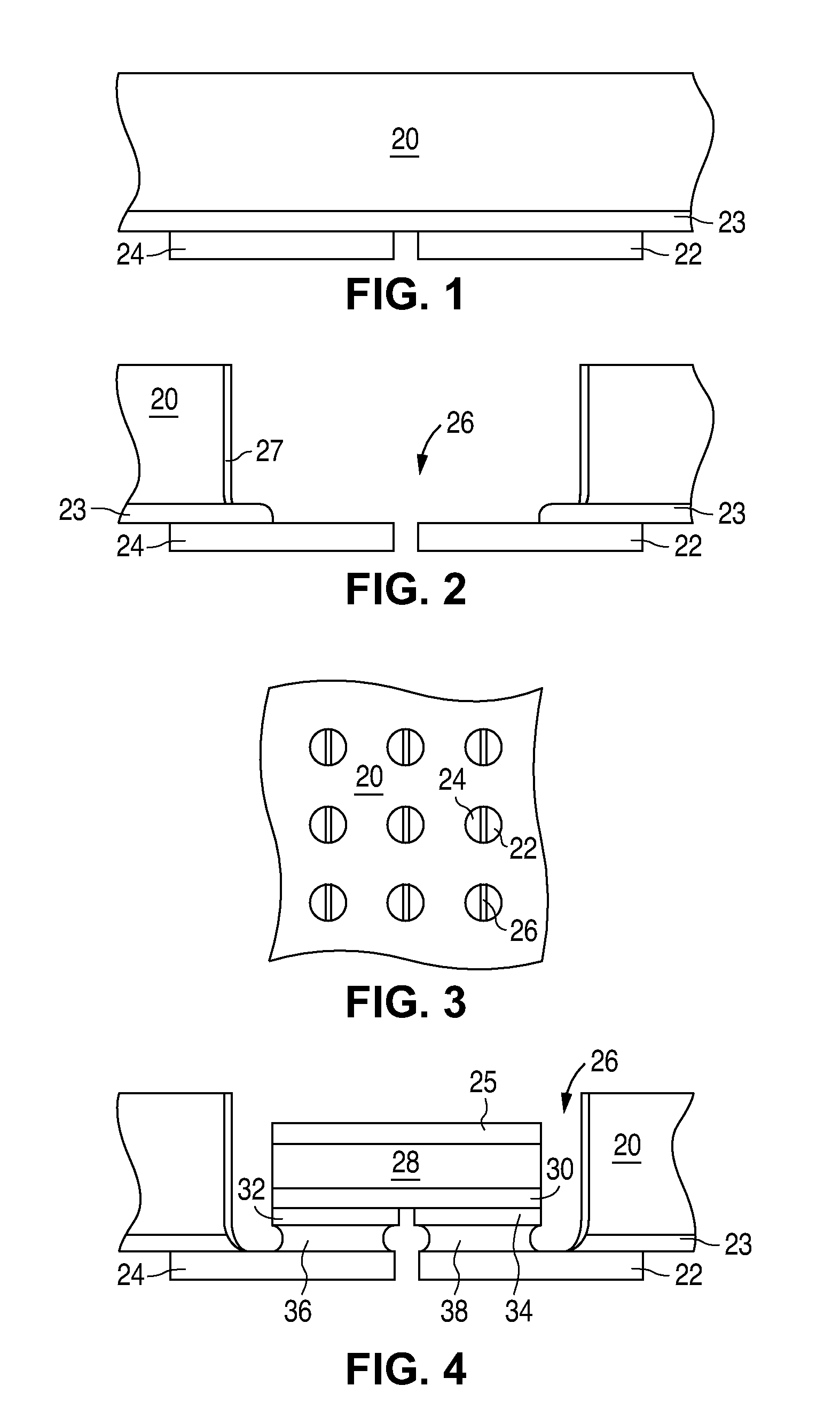
[0020]In the structure illustrated in FIG. 1, metal leads 22 and 24 are formed on one side of a carrier 20. The material of carrier 20 is selected for the strength to withstand required processing and bonding steps, for ease of handling during any processing steps such as machining, and for ease of patterning during patterning steps. Carrier 20 may be, for example, silicon, other semiconductors such as GaAs, GaP, or Ge, or a non-semiconductor such as plastic, alumina, ceramic, a fluoropolymer such as polytetrafluoroethylene (Teflon®), polycrystalline materials, or glass. In some embodiments, carrier 20 may be flexible. In some embodiments, wavelength converting or luminescent materials such as phosphor may be incorporated in carrier 20.

[0021]In some embodiments, leads 22 and 24 are electrically isolated from carrier 20 by a nonconductive layer 23, which may be, for example, an oxide of silicon. Nonconductive layer 23 may be formed on the bottom surface of carrier 20 prior to forming...


PUM


Abstract

A mount for a semiconductor device includes a carrier, at least two metal leads disposed on a bottom surface of the carrier, and a cavity extending through a thickness of the carrier to expose a portion of the top surfaces of the metal leads. A semiconductor light emitting device is positioned in the cavity and is electrically and physically connected to the metal leads. The carrier may be, for example, silicon, and the leads may be multilayer structures, for example a thin gold layer connected to a thick copper layer.

Description

BACKGROUND[0001]1. Field of Invention[0002]The present invention is directed to a mount for a semiconductor light emitting device such as a light emitting diode.[0003]2. Description of Related Art[0004]Semiconductor light emitting devices such as light emitting diodes (LEDs) are among the most efficient light sources currently available. Material systems currently of interest in the manufacture of high brightness LEDs capable of operation across the visible spectrum include group III-V semiconductors, particularly binary, ternary, and quaternary alloys of gallium, aluminum, indium, and nitrogen, also referred to as III-nitride materials; and binary, ternary, and quaternary alloys of gallium, aluminum, indium, arsenic, and phosphorus. Often III-nitride devices are epitaxially grown on sapphire, silicon carbide, or III-nitride substrates and III-phosphide devices are epitaxially grown on gallium arsenide by metal organic chemical vapor deposition (MOCVD), molecular beam epitaxy (MBE),...

Claims


Application Information

Patent Timeline
Patent Type & Authority Applications(United States)
IPC IPC(8): H01L33/00H01L33/62H01L33/64
CPCH01L33/62H01L33/642H01L33/647H01L2224/16H01L2224/0554H01L2224/05568H01L2224/05573H01L2224/056H01L2924/00014H01L2224/05599H01L2224/0555H01L2224/0556
Inventor CRAFORD, M. GEORGEKRAMES, MICHAEL R.
Owner PHILIPS LUMILEDS LIGHTING CO LLC
Why Eureka
Try Eureka