Semiconductor device and method of manufacturing the same

a technology of semiconductors and components, applied in the direction of optics, transistors, instruments, etc., can solve the problems of large resistance of the plug conspicuously, reduce the diameter of the plug (contact plug) to connect the misfet and the wire of the lcd driver, and reduce the resistance of the plug. , the effect of large aspect ratio of the plug

Active Publication Date: 2008-12-11
RENESAS ELECTRONICS CORP
View PDF3 Cites 37 Cited by
  • Summary
  • Abstract
  • Description
  • Claims
  • Application Information

AI Technical Summary

Benefits of technology

[0008]In recent years, miniaturization of the LCD driver is demanded. For this purpose, a diameter of the plug (contact plug) to connect the MISFET and the wire of the LCD driver is reduced. For example, concretely, the diameter of the plug is largely reduced to 0.24 μm or 0.14 μm. However, when the diameter of the plug is reduced, a problem that the resistance of the plug becomes large conspicuously occurs. In particular, in the high voltage resistant MISFET, since the high voltage resistant MISFET and the wire are connected each other by the plug penetrating both the interlayer insulation film of the first layer and the interlayer insulation film of the second layer, when the diameter of the plug is reduced, an aspect ratio of the plug becomes large and the resistance increases. Therefore, in the LCD driver, the wire is formed on the interlayer insulation film of the first layer, and a wire width of the wire formed on the interlayer insulation film of the first layer is made wide and the number of plugs to connect the interlayer insulation film of the first layer and the interlayer insulation film of the second layer is increased, whereby the low resistance of the plug is secured. By forming the wire on the interlayer insulation film of the first layer, there is no need to directly connect the plug penetrating the interlayer insulation film of the first layer and the plug that penetrates the interlayer insulation film of the second layer, so that the aspect ratio of the plug can be reduced. Therefore, the high resistance due to reduction of the plug diameter can be suppressed.
[0009]Further, by thinning a film thickness of the interlayer insulation film of the first layer, the aspect ratio of the plug formed in the interlayer insulation film of the first layer is made small. In this manner, in chip shrinking of the LCD driver, the film thickness of the interlayer insulation film of the first layer is made thin, and the wire is formed on the interlayer insulation film of the first layer. The wire width of the wire formed on the interlayer insulation film of the first layer is made wide, and the number of plugs to connect the interlayer insulation film of the first layer and the interlayer insulation film of the second layer is increased. Since the wire width of the wire formed on the interlayer insulation film of the first layer is made wide, a source wire to be connected to the source region of the high voltage resistant MISFET or a drain wire to be connected to the drain area of the high voltage resistant MISFET is formed so as to have a region which is planarly overlapped with the gate electrode of the high voltage resistant MISFET.

Problems solved by technology

However, when the diameter of the plug is reduced, a problem that the resistance of the plug becomes large conspicuously occurs.

Method used


Image

  • Semiconductor device and method of manufacturing the same
  • Semiconductor device and method of manufacturing the same
  • Semiconductor device and method of manufacturing the same

Examples


first embodiment

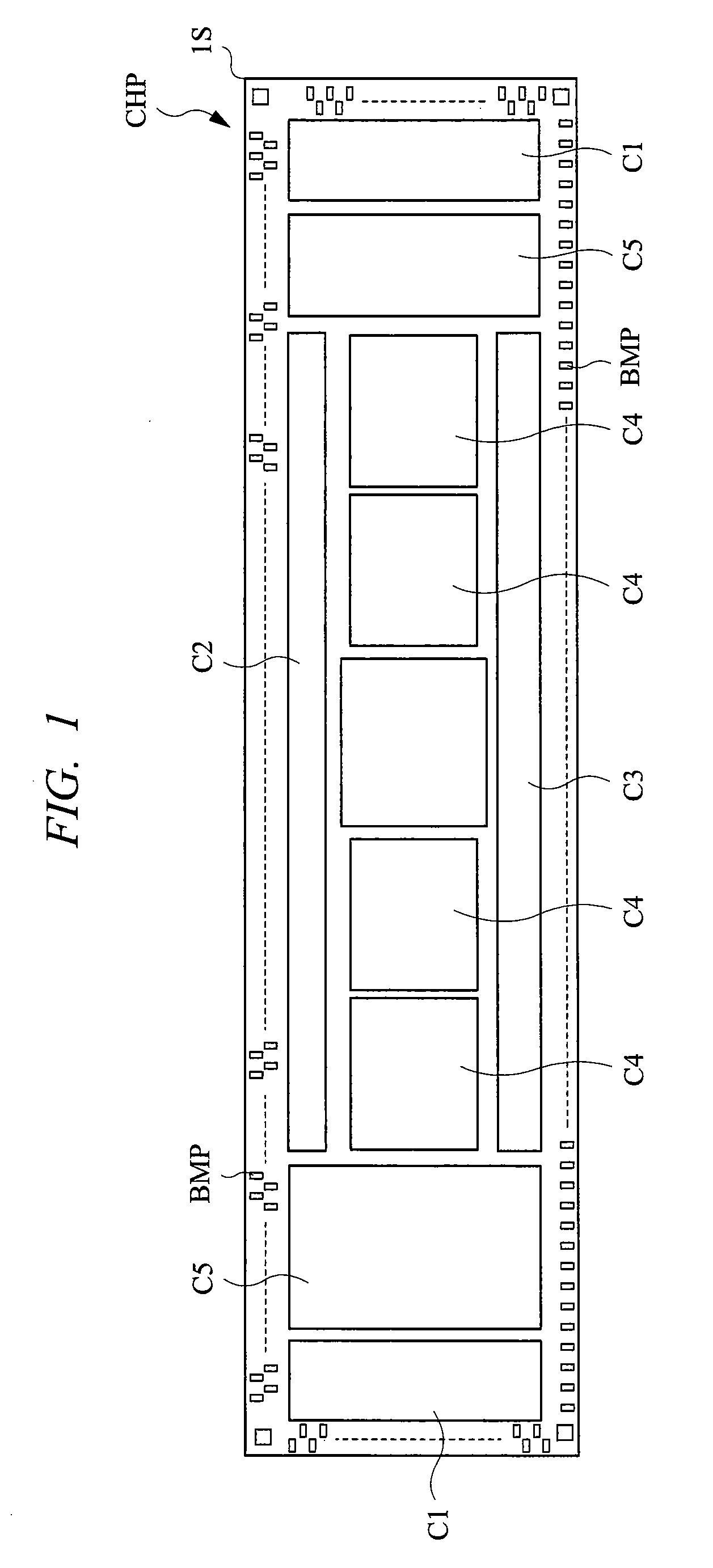
[0069]First, a semiconductor chip for an LCD driver according to the present embodiment will be explained. FIG. 1 is a plan view showing a structure of a semiconductor chip CHP (semiconductor device) according to the present embodiment. The semiconductor chip CHP according to the present embodiment is an LCD driver. In FIG. 1, the semiconductor chip CHP has a semiconductor substrate 1S formed into, for example, an elongated rectangle shape, and the LCD driver to drive, for example, a liquid crystal display device is formed on a main surface of the semiconductor substrate 1S. This LCD driver has a function to supply a voltage to each pixel of cell arrays constituting the LCD and control directions of liquid crystal molecules, and includes gate drive circuits C1, a source drive circuit C2, a liquid crystal drive circuit C3, graphic Random Access Memories (RAM) C4 and peripheral circuits C5.

[0070]In the vicinity of the outer circumference of the semiconductor chip CHP, a plurality of b...

second embodiment

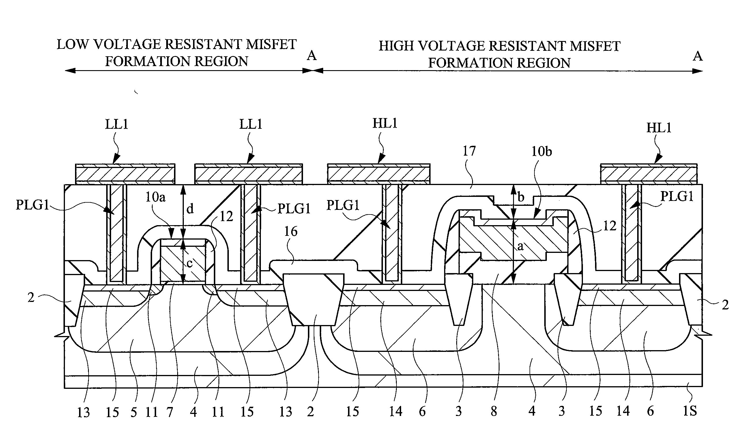
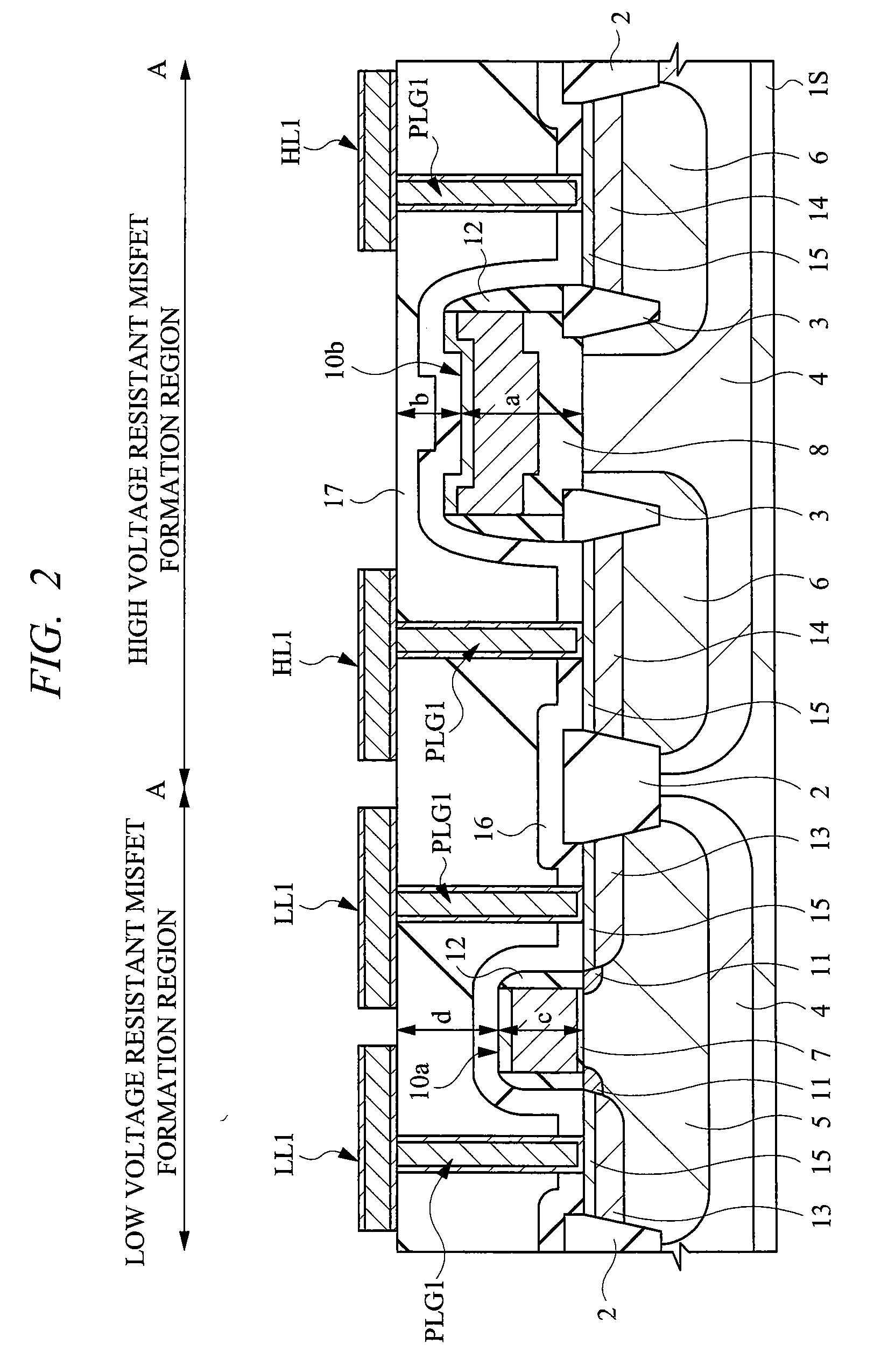
[0150]One of the characteristics of the first embodiment lies in, as shown in FIG. 28, a point where the wires HL1 to become the source wire and the drain wire are formed on the insulation film (silicon oxide film 17) of the first layer, and the wires HL1 are arranged so that the wires HL1 and the gate electrode 10b of the high voltage resistant MISFET should not be overlapped planarly. In FIG. 28, a distance “e” of an interval in which the gate electrode 10b of the high voltage resistant MISFET and the wires HL1 are not overlapped planarly is shown, and in a second embodiment, specific numerical value examples of this distance “e” will be explained.

[0151]FIG. 28 is a cross sectional view showing the high voltage resistant MISFET and the low voltage resistant MISFET, and it is a figure similar to FIG. 2. However, in FIG. 28, the distance “e” of the interval where the gate electrode 10b and the wires HL of the high voltage resistant MISFET are not overlapped planarly, and a diameter ...

third embodiment

[0157]In the first embodiment, it is characteristic that the wires HL1 formed on the interlayer insulation film of the first layer (silicon oxide film 17) and the gate electrode 10b of the high voltage resistant MISFET shown in FIG. 28 are arranged not to be overlapped planarly. In other words, in the first embodiment, attention is paid to a problem caused by thinning the interlayer insulation film of the first layer, and is paid to the fact that the voltage resistance between the wires HL1 formed in the interlayer insulation film of the first layer and the gate electrode 10b becomes the problem caused by thinning the insulation film of the first layer. At this moment, in the first embodiment, it is quantitatively defined that the interlayer insulation film of the first layer is thinned.

[0158]In concrete, as shown in FIG. 28, when the distance from the interface between the semiconductor substrate 1S and the gate insulation film 8 to the upper portion of the gate electrode 10b is de...


PUM

PropertyMeasurementUnit
drive voltageaaaaaaaaaa
distanceaaaaaaaaaa
voltageaaaaaaaaaa

Abstract

In an LCD driver, in a high voltage resistant MISFET, end portions of a gate electrode run onto electric field relaxing insulation regions. Wires to become source wires or drain wires are formed on an interlayer insulation film of the first layer over the high voltage resistant MISFET. At this moment, when a distance from an interface between a semiconductor substrate and a gate insulation film to an upper portion of the gate electrode is defined as “a”, and a distance from the upper portion of the gate electrode to an upper portion of the interlayer insulation film on which the wires are formed is defined as “b”, a relation of a>b is established. In such a high voltage resistant MISFET structured in this manner, the wires are arranged so as not to be overlapped planarly with the gate electrode of the high voltage resistant MISFET.

Description

CROSS-REFERENCE TO RELATED APPLICATION[0001]The present application claims priority from Japanese Patent Application No. JP 2007-153840 filed on. Jun. 11, 2007, and No. JP 2008-71291 filed on Mar. 19, 2008, the content of which is hereby incorporated by reference into this application.TECHNICAL FIELD OF THE INVENTION[0002]The present invention relates to a semiconductor device and a method of manufacturing the same, and particularly, it relates to an effective technology when applied to a semiconductor device equipped with a relatively high voltage resistant MISFET such as a Liquid Crystal Display (LCD) driver and the like and a method of manufacturing the same.BACKGROUND OF THE INVENTION[0003]In Japanese Patent Application Laid-Open Publication No. 2005-116744 (Patent Document 1), a technology of forming a high voltage resistant transistor and a low voltage resistant transistor on a same substrate is described. In this Patent Document 1, it is said that the high voltage resistant t...

Claims


Application Information

Patent Timeline
Patent Type & Authority Applications(United States)
IPC IPC(8): G02F1/136H01L21/336H01L29/78
CPCH01L21/76229H01L21/76837H01L21/823456H01L21/823462H01L21/823475H01L21/823481H01L23/53295H01L2924/0002H01L29/0653H01L29/7836H01L29/66477H01L2924/00H01L23/50H01L27/088G02F1/133302G02F1/136295H01L23/535H01L29/78G02F1/13306G02F1/133345G02F1/134309G02F1/13439G02F1/136286G02F1/1368H01L21/02274H01L21/31051H01L21/76224H01L21/76895H01L27/124H01L29/6675
Inventor TERADA, YUSUKETOYOKAWA, SHIGEYAMAEDA, ATSUSHI
Owner RENESAS ELECTRONICS CORP
Why Eureka
Try Eureka