

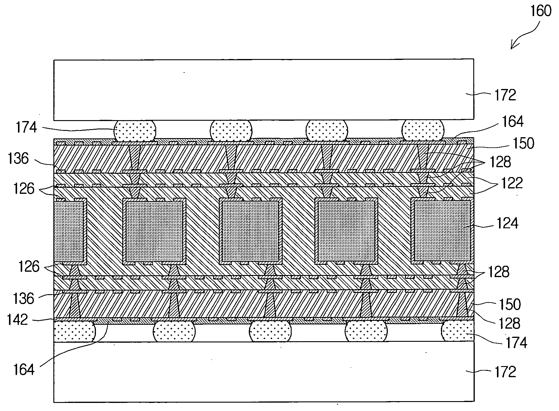
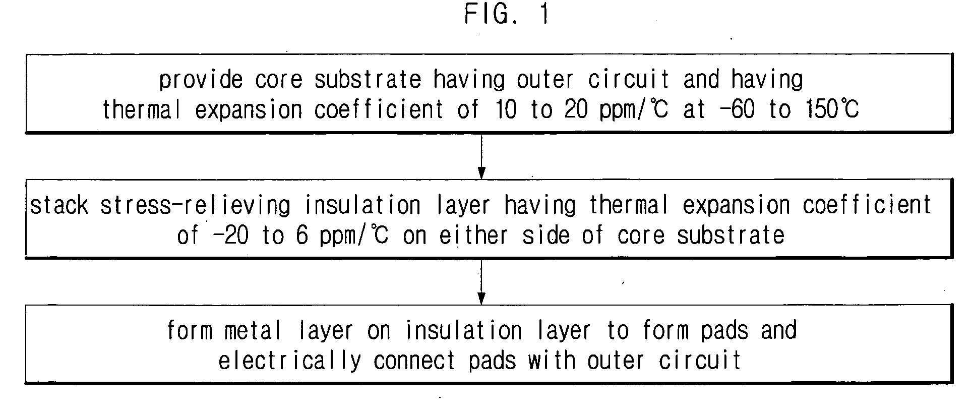
Multilayered printed circuit board and fabricating method thereof
a printed circuit board and multi-layer technology, applied in the direction of printed circuit aspects, printed circuit stress/warp reduction, semiconductor/solid-state device details, etc., can solve the problems of defect risk, peeling, cracking, and damage of semiconductor chips, and achieve high contact reliability
- Summary
- Abstract
- Description
- Claims
- Application Information
AI Technical Summary
Benefits of technology
Problems solved by technology
Method used
Image

Examples
implementation example 1
[0086](1) Fabrication of Core Substrate
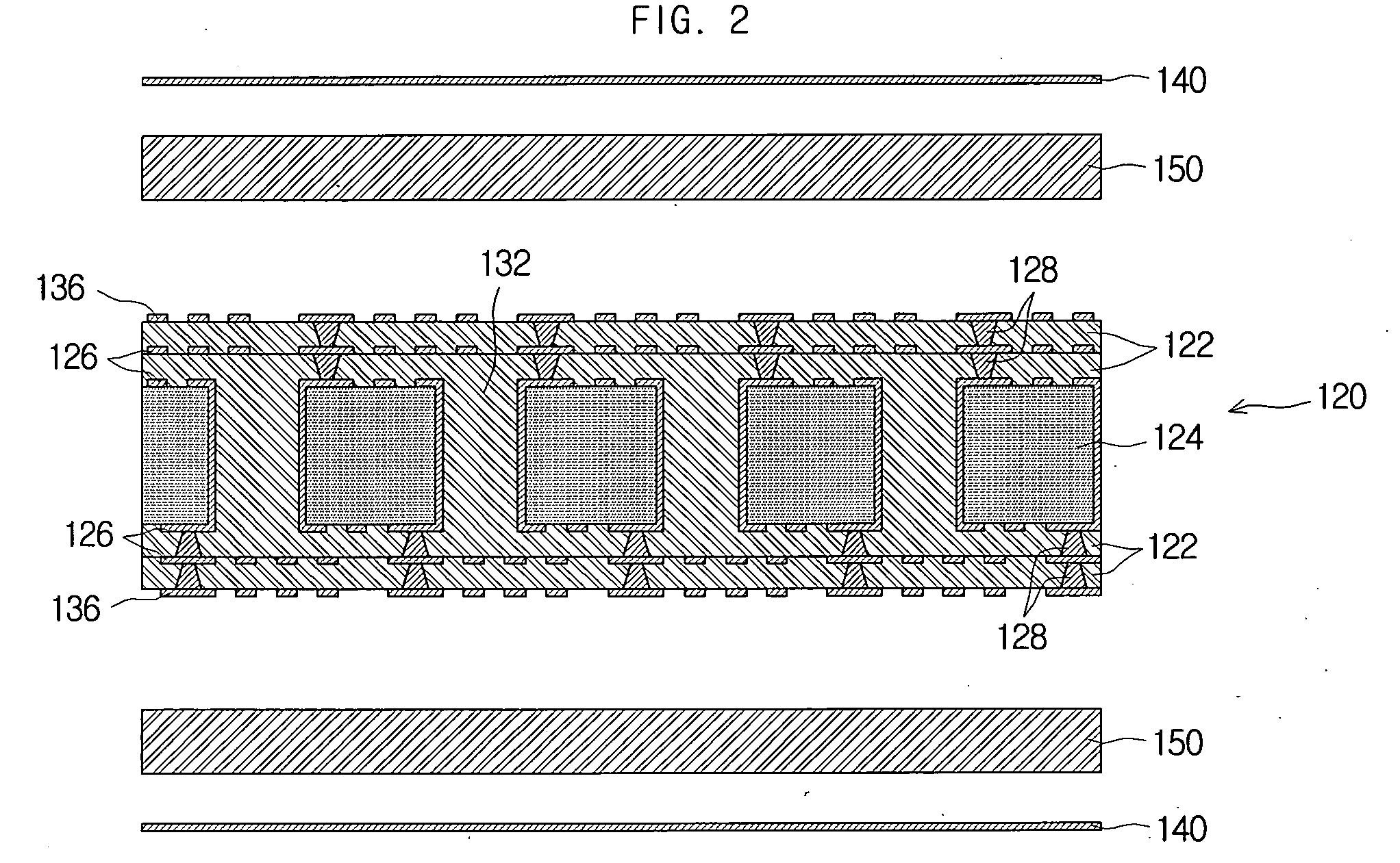
[0087]To a copper clad laminate (product name: ELC-4785 GS, CTEα1: 11 ppm / ° C., Sumitomo Bakelite Co., Ltd.) having a 12 μm-thick electro-deposited copper layer attached on either side of a 0.2 mm-thick insulation layer of epoxy, the copper of the surface layers were etched to a thickness of 1.3 μm. Then, through-holes were formed using a metal drill to an inner diameter of 150 μm, and desmearing was performed, after which an electroless plating copper layer of 0.9 μm and an electroplating copper layer of 20 μm were applied. Afterwards, circuits were formed by a subtractive method to a ratio of line / space=40 / 40 μm, and black copper oxide treatment was performed. Then, a build-up sheet (product name: APL-3601, Sumitomo Bakelite Co., Ltd.) of 40 μm thickness was applied on either side, a 12 μm-thick electro-deposited copper layer was arranged on either outer side, and stack-molding was performed for 90 minutes in a 200° C., 25 kgf / cm2, and 2 mmHg...
implementation example 2
[0093](1) Fabrication of Core Substrate
[0094]2,2-Bis(4-cyanatophenyl)propane monomers of 550 parts were dissolved at 160° C. and were reacted while being stirred for 4.5 hours, to yield a mixture of monomers and prepolymers. These were dissolved in methyl ethyl ketone and mixed with 100 parts of bisphenol A epoxy resin (product name: Epikote 1001, Japan Epoxy Resins Co., Ltd.), 150 parts of phenol novolac epoxy resin (product name: DEN-431, Dow Chemical Company), and 200 parts of cresol novolac epoxy resin (product name: ESCN-220 F, Sumitomo Chemical Co., Ltd.), after which 0.2 parts of zinc octylate was dissolved as a hardening catalyst in the methyl ethyl ketone. The mixture was mixed and stirred to form Varnish-D. Then, 1000 parts of spherical silica (average particle diameter: 0.9 μm) inorganic filler was added, stirred, and dispersed to form Varnish-E.
[0095]Varnish-D was impregnated into a 200 μm-thick aramid fiber woven fabric and dried, to fabricate Prepreg-F having a gelatio...
implementation example 3
[0103](1) Fabrication of Core Substrate
[0104]First, a core substrate was prepared by performing the processes described as in (1) of Implementation Example 2.
[0105](2) Fabrication of Multilayered PCB
[0106]Varnish-E was impregnated into a 100 μm-thick T(S) glass fiber woven fabric and dried, to fabricate Prepreg-M having a gelation time of 117 seconds and a resin content of 55 weight %. Then, a sheet of T(S) glass fiber woven fabric Prepreg M (CTEα1 after hardening: 5.3 ppm / ° C.) was placed each on both sides of PCB-J, and 12 μm-thick electro-deposited copper layers were arranged on the outer sides, which were stack-molded for 90 minutes in a 190° C., 40 kgf / cm2, 2 mmHg vacuum, to fabricate an eight-layer copper clad stack. After removing the copper layers on the surfaces to a thickness of 1.5 μm by etching, blind via holes of a 70 μm diameter were formed on both sides using UV-YAG laser. Then, the blind via holes were subjected to a desmearing treatment using plasma, and the insides...
PUM
| Property | Measurement | Unit |
|---|---|---|
| melting point | aaaaa | aaaaa |
| thickness | aaaaa | aaaaa |
| thickness | aaaaa | aaaaa |
Abstract
Description
Claims
Application Information