
GaInNAsSb solar cells grown by molecular beam epitaxy

a solar cell and molecular beam technology, applied in the field of solar cell technology, can solve the problems of poor performance, difficult manufacturing of lattice-matched structures, and poor efficiency of most dilute nitride solar cells, and achieve the effects of promoting efficient solar energy conversion, high efficiency, and favorable characteristics of solar cells

Inactive Publication Date: 2009-01-15
CACTUS MATERIALS INC +1
View PDF33 Cites 103 Cited by
  • Summary
  • Abstract
  • Description
  • Claims
  • Application Information

AI Technical Summary

Benefits of technology

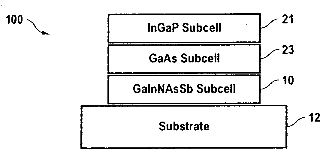
[0011]According to the invention, a high efficiency triple-junction solar cell and method of manufacture therefor is provided wherein junctions are formed between different types of III-V semiconductor alloy materials formed in subcells, one alloy of which contains a combination of an effective amount of antimony (Sb) with gallium (Ga), indium (In), nitrogen (N, the nitride component) and arsenic (As) to form the dilute nitride semiconductor layer or subcell GaInNAsSb which has particularly favorable characteristics in a solar cell. An effective amount of antimony has been determined to be between about 2% and 6%. In particular, the bandgap and lattice matching promote efficient solar energy conversion.
[0012]In one aspect of the invention, a method of manufacturing using molecular beam epitaxy is provided, wherein voltage-biased deflection plates that are disposed at the front of a nitrogen plasma cell in an MBE system can reduce the number of ions impinging on the dilute nitride epilayer as it is being grown. Other design parameters that can be selected to reduce the ion flux at the epilayer include: the number and / or size of holes at the front aperture of the plasma cell, the location and / or pattern of these holes, RF power delivered to the source and gas pressure in the source. Since ions impinging on the epilayer being grown can damage the epilayer and introduce defects, it is significantly advantageous to reduce the incident ion flux during growth.
[0013]In a second aspect of the invention, compositional and phase segregation are reduced, and native defect concentration is also reduced in dilute nitrides, thereby improving carrier lifetime and diffusion length. The resulting dilute nitrides can have improved surface quality and can provide increased efficiency in solar cells. The antimony (Sb) is believed to serve as a surfactant, and a low percentage (<10%) constituent can improve the quality of dilute nitrides. Specifically, addition of antimony (Sb) reduces the propensity of indium (In) and nitrogen (N) to segregate during growth and also inhibits 3-D growth. As a result, a higher temperature growth window is made available providing fewer native defects. The resulting grown material has superior transport and p-n junction properties.
[0014]In a third aspect of the invention, an epitaxially grown dilute nitride antimonide layer is lattice matched to a GaAs or Ge substrate and has a bandgap of 0.9 eV to 1.1 eV. Such a layer can be the ˜1 eV junction of a high efficiency multi-junction solar cell. More specifically, GaNAsSb or GaInNAsSb can be grown with a set of compositions that provide a bandgap of 0.9 eV to 1.1 eV together with lattice matching to GaAs or Ge. This layer can be part of a multi-junction solar cell, absorbing light having energy ˜1 eV and greater. This material composition for the 1 eV layer can provide reduced defect density compared to conventional approaches based on an InGaAs 1 eV layer. Reduction of defect density can increase cell efficiency.

Problems solved by technology

To date most dilute nitride solar cells have been plagued with poor efficiency, due presumably to short diffusion lengths.
These materials can raise device efficiency without the need for metamorphic structures, which inherently contain many defects in the graded region, are generally thicker due to the graded buffer layer, and are more difficult to manufacture than lattice-matched structures.
691-694) to be plagued with poor performance due to short diffusion lengths coupled with narrow depletion widths.

Method used


Image

  • GaInNAsSb solar cells grown by molecular beam epitaxy
  • GaInNAsSb solar cells grown by molecular beam epitaxy
  • GaInNAsSb solar cells grown by molecular beam epitaxy

Examples


Embodiment Construction

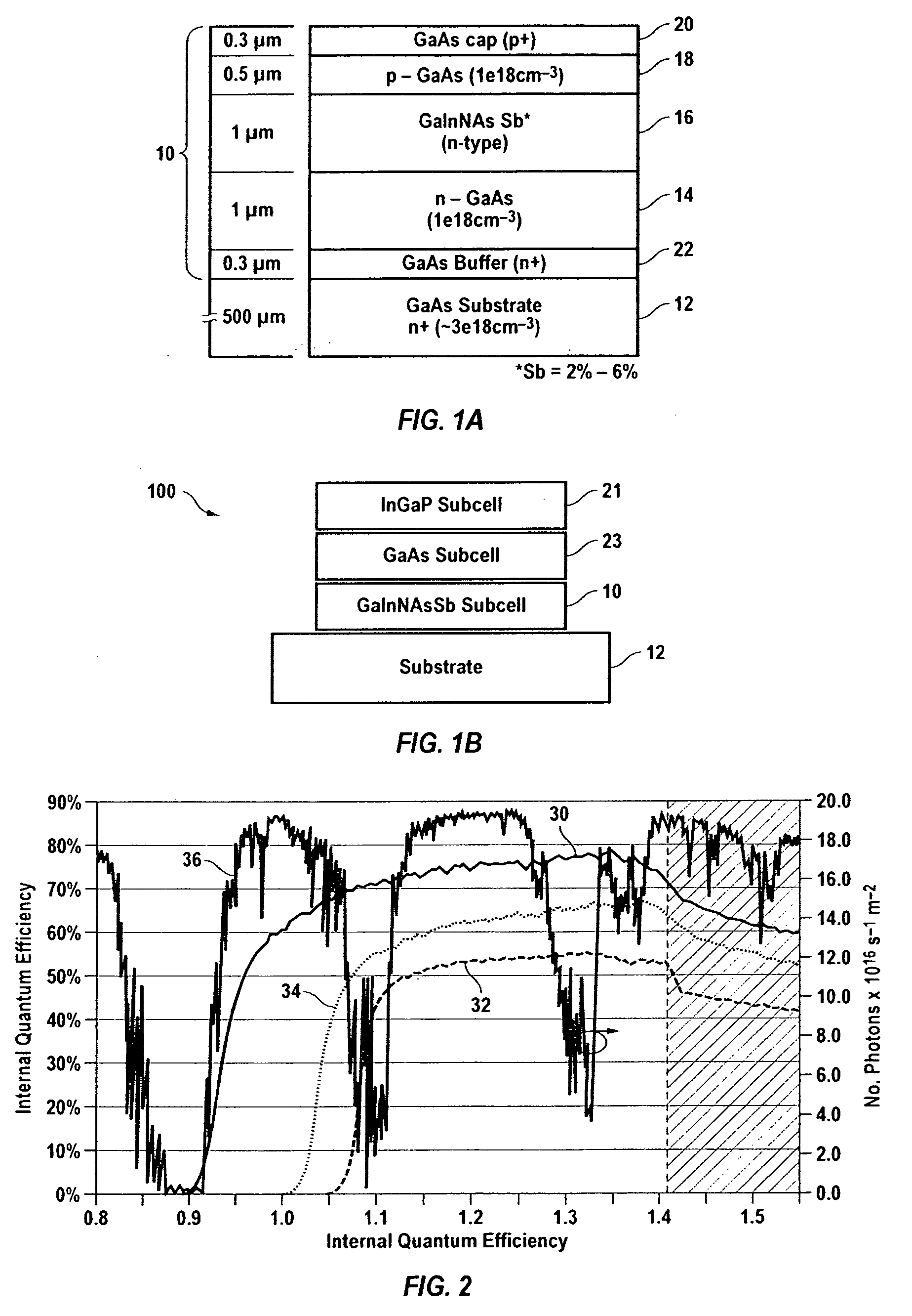
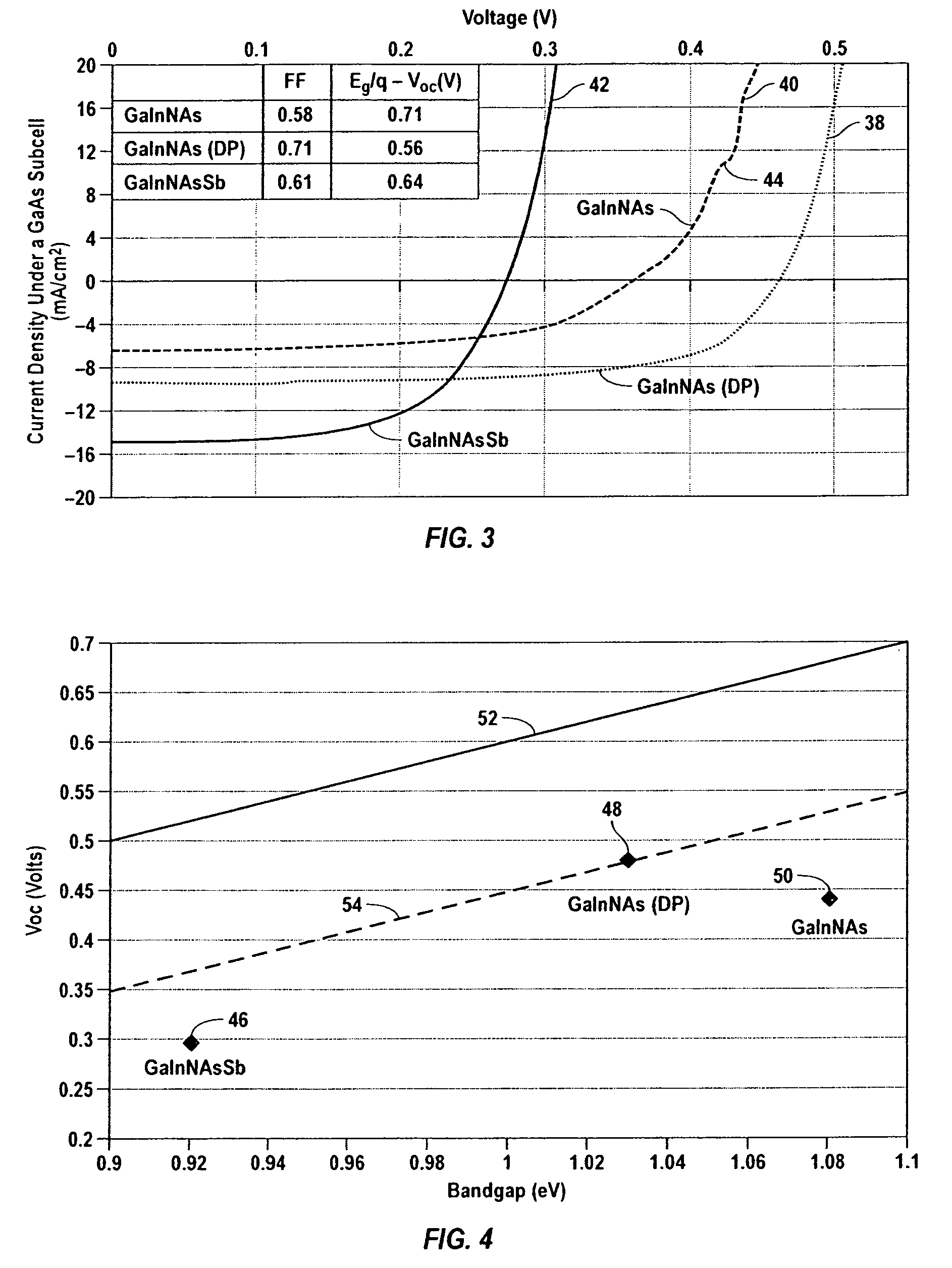
[0025]Two techniques have been explored that have been aimed at improving the quality of thicker narrow band gap, nearly lattice-matched III-V type dilute nitride films in solar cells grown by molecular beam epitaxy (MBE), namely the utilization of biased deflection plates installed in front of the nitrogen plasma source, and the introduction of antimony to the growth process. The experimental results indicate that antimony-containing nitride films above certain concentrations actually improved performance of solar cells, in contrast to prior art teachings that the presence of antimony was deleterious to the achievement of desired characteristics useful in a solar cell.

[0026]According to the invention and in reference to FIGS. 1A and 1B, a material system 10, herein a layer, which contains a dilute nitride film (FIG. 1A), that specifically contains antimony in the nitride film, namely, GaInNAsSb 16 with approximately 2% to 6% antimony (“Sb”), can be grown on a substrate 12 that is s...


PUM


Abstract

A high efficiency triple-junction solar cell and method of manufacture therefor is provided wherein junctions are formed between different types of III-V semiconductor alloy materials, one alloy of which contains a combination of an effective amount of antimony (Sb) with gallium (Ga), indium (In), nitrogen (N, the nitride component) and arsenic (As) to form the dilute nitride semiconductor layer GaInNAsSb which has particularly favorable characteristics in a solar cell. In particular, the bandgap and lattice matching promote efficient solar energy conversion.

Description

CROSS-REFERENCES TO RELATED APPLICATIONS[0001]This application claims benefit under 35 U.S.C. § 119(e) of Provisional Patent Application 60 / 959,043 filed Jul. 10, 2007 entitled Improved Carrier Lifetime and Mobility in Dilute Nitrides Grown by MBE Via Ion Count Reduction, the content of which is incorporated herein for all purposes.STATEMENT AS TO RIGHTS TO INVENTIONS MADE UNDER FEDERALLY SPONSORED RESEARCH OR DEVELOPMENT[0002]This material is based on work supported by the NSF under Grants No. 9900793 and No. 0140297, with imaging and measurements carried out by NREL under Contract No. DE-AC36-99GO10337 with the U.S. Department of Energy. The subject matter herein described is subject to a government license in connection with Leland Stanford Junior University.REFERENCE TO A “SEQUENCE LISTING,” A TABLE, OR A COMPUTER PROGRAM LISTING APPENDIX SUBMITTED ON A COMPACT DISK[0003]Not ApplicableBACKGROUND OF THE INVENTION[0004]This invention relates to solar cell technology and in particu...

Claims


Application Information

Patent Timeline
IPC IPC(8): H01L31/00
CPCH01L31/0304H01L31/03046H01L31/0687H01L31/0693Y02E10/544H01L31/078H01L31/1844H01L31/1852H01L31/0725Y02P70/50
Inventor HARRIS, JR., JAMES S.YUEN, HOMAN B.BANK, SETH R.WISTEY, MARK A.JACKREL, DAVID B.
Owner CACTUS MATERIALS INC
Learn More