Multilayer wiring structure and method of manufacturing the same

a multi-layer wiring and manufacturing method technology, applied in the direction of resistive material coating, printed circuit assembling, non-metallic protective coating application, etc., can solve the problems of increasing contact resistance, reducing long-term reliability of printed boards and ceramic substrates, and voids and air bubbles that remain, so as to achieve small voltage loss and high potential

Inactive Publication Date: 2009-01-29
RICOH KK
View PDF6 Cites 46 Cited by
  • Summary
  • Abstract
  • Description
  • Claims
  • Application Information

AI Technical Summary

Benefits of technology

[0067]Since the via post is in contact at the head or the side surface thereof with the pixel electrode, contact resistance between the pixel electrode and the source or drain electrode connected through the via post is very low.
[0068]Therefore, if any one of TFTs is...

Problems solved by technology

However, if the diameter of the via hole is as small as about 100 μm, air in the via hole is not completely removed by the conductive paste, so that unwanted air bubbles and voids remain in the via hole filled with the conductive paste.
As a result, the contact resistance of the via hole is increased, which lowers output signal and frequency properties.
The increase of contact resistance lowers long-term reliability of the printed boards and ceramic substrates.
As the viscosity increases, removal of the air bubbles and gaps by vibration becomes more difficult and incomplete.
It seems that this method cannot be used for filling a via hole having a diameter smaller than 100 μm.
Another problem with this method is that a special heating oven is required for generating vibration of 1-100 Hz.
Therefore, it seems to be difficult to fill via holes smaller than conventional via holes by using the method of Patent Document 2.
A common problem for the methods disclosed in Patent Documents 3 and 4 is that dust is generated during the polishing process for exposing the head of the columnar conductor 46 (the capacitor paste and the plating metal), and the dust might cause contact failure if deposited on an interface between the columnar conductor 46 (the capacitor paste and the plating metal) and the upper metal wiring element 49.
A cleaning process is therefore added after the mechanical polishing process, making the manufacturing process more complex.
Moreover, polishing machines and cleaning machines increase the cost of manufacturing equipment.
As can be seen from the above description, filling small via holes is a big challenge in manufacturing printed boards and ceramic substrates having multilayer wiring structures.
However, the active matrix drive circuits also have multilayer wiring structures, and there are almost no techniques for printing a via hole with a diameter as small as about 50-100 μm in interlayer insulation films.
Moreover, techniques for filling holes of 50-100 μm with conductive paste are not yet established as in the case of the printed wiring boards and the ceramic substrates.
Since the emulsion pattern may possibly come off during production of the screen mask, it is very difficult to produce the screen mask having no defects.
Thus, the life of the screen mask is much shorter compared to conventional screen masks.
As can be seen, manufacturing a defective-free and long-life screen mask for forming via holes as well as completely filling small via holes with a conductive paste are big technical problems in forming active matrix drive circuits by screen printing in the production process of the flat panel displays.
Although crystalline organic semiconductors such as pentacene have high mobility and are therefore promising in terms of high speed drive, the crystalline organic semiconductors are disadvantageous in that production of large-size and uniform semiconductor...

Method used


Image

  • Multilayer wiring structure and method of manufacturing the same
  • Multilayer wiring structure and method of manufacturing the same
  • Multilayer wiring structure and method of manufacturing the same

Examples


embodiment 1

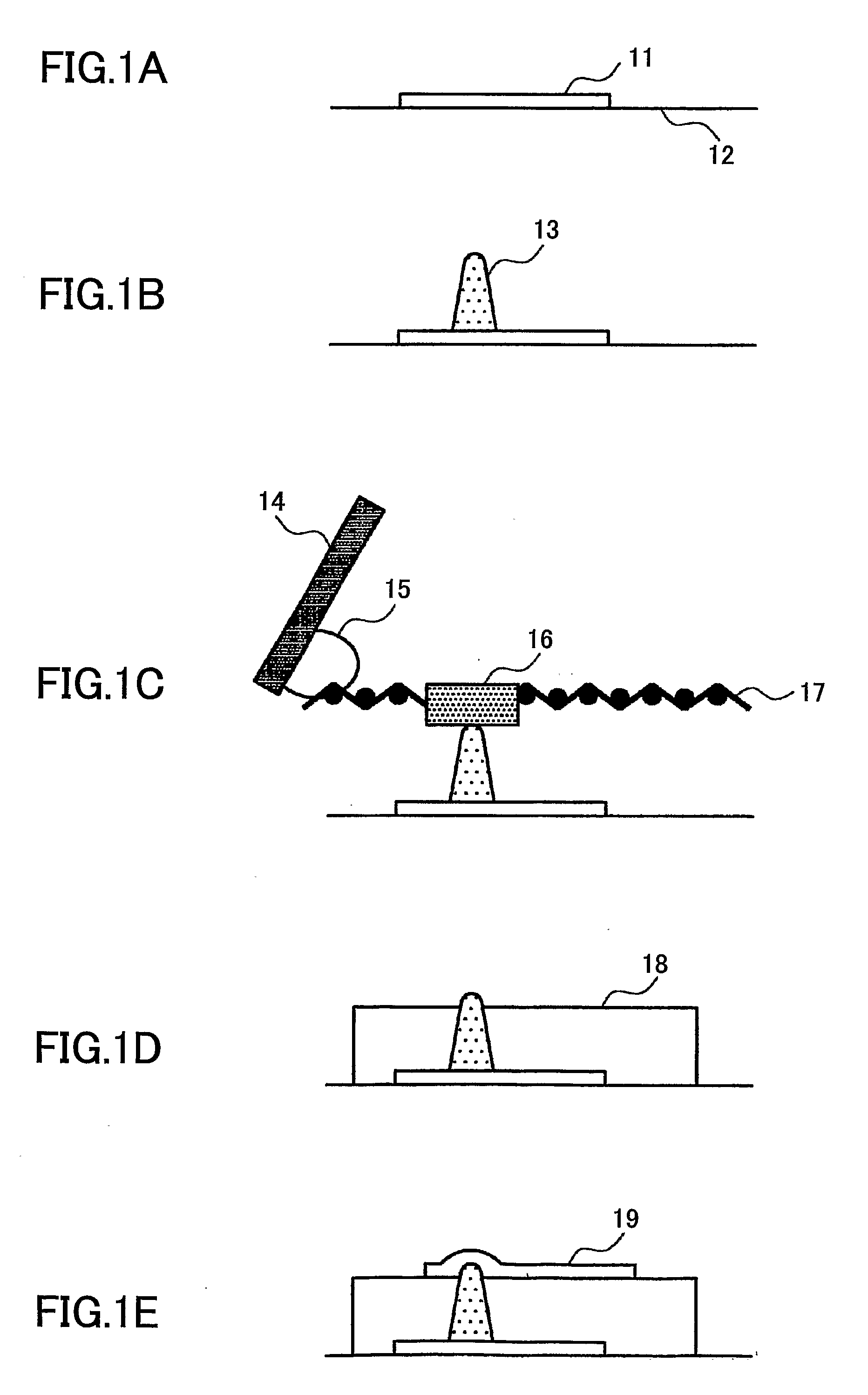
[0118]FIGS. 1A-1E illustrate a method of manufacturing a multilayer wiring structure according to Embodiment 1 of the present invention.

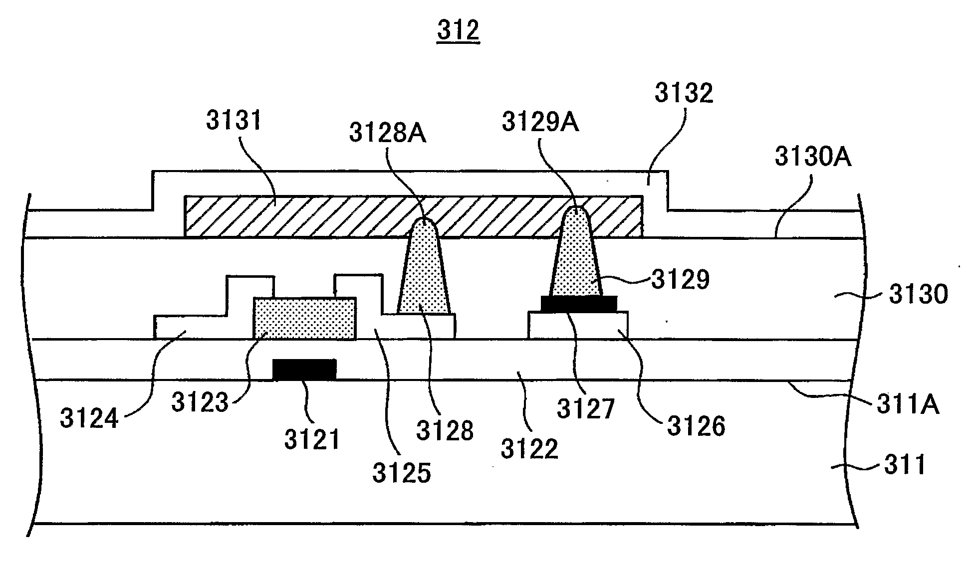
[0119]In the step shown in FIG. 1A, a first metal wiring element 11 is formed on a glass substrate 12 using a screen printing method. A conductive paste used herein for printing is an Ag paste that contains Ag particles, acrylic resin, carbitol acetate, etc., and has a viscosity of 100-220 Pa·s. It is to be noted that the viscosity measurement is performed at 10 rpm using Brookfield HBT No. 14 spindle at room temperature. These conditions are applied to other viscosity measurements that follow. A screen mask used herein is a stainless mesh No. 500 with an emulsion thickness of 8 μm. The first metal wiring element 11 having a width of 50 μm is printed with the Ag paste, using the above screen mask and a squeegee 14 having a rubber hardness of 70. The land diameter of a via hole through which the first metal wiring element 11 and a second metal wiring...

embodiment 2

[0144]The following describes Embodiment 2, again with reference to FIGS. 1A-1E.

[0145]In the same way as in Embodiment 1, a first metal wiring element 11 (having a width of 50 μm and a land diameter of 150 μm) is formed on a glass substrate 12, and then a via post 13 is formed on a land of the first metal wiring element 11. The via post 13 has a head size of 50-60 μm and a height of 11-13 μm.

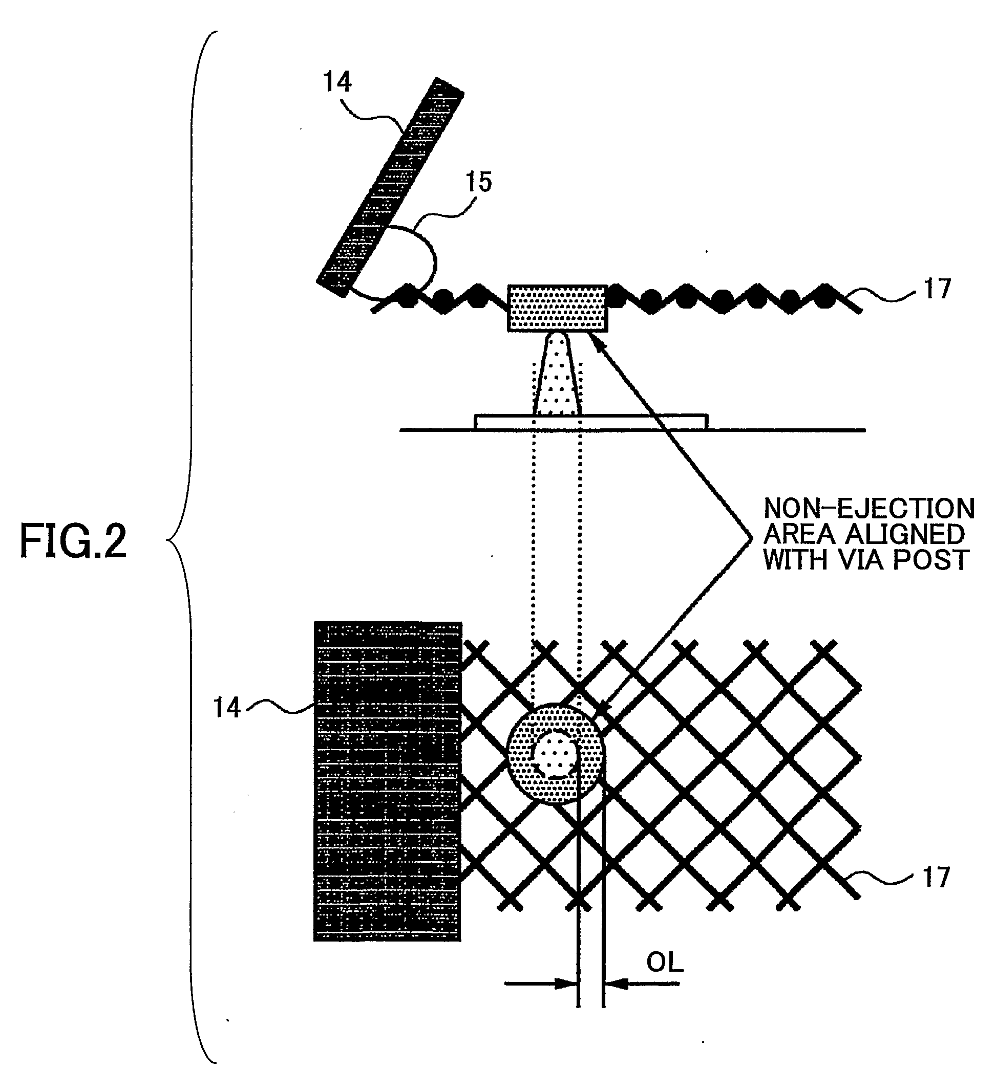
[0146]After that, an insulation paste 15 is printed by screen printing and cured by heating so as to form an interlayer insulation film 18. A screen mask 17 used herein has a non-ejection area 16. The design rule of a distance OL between the non-ejection area 16 and the via post 13 with one side is in a range of 10-50 μm. An insulation paste 15 and a squeegee 14 used in Embodiment 2 are the same as those in Embodiment 1.

[0147]Then, in the same way as in Embodiment 1, a second metal wiring element 19 (having a width of 100 μm and a land diameter of 150 μm) is formed on the surface of the interlay...

embodiment 3

[0154]The following describes Embodiment 3, again with reference to FIGS. 1A-1E.

[0155]In the same way as in Embodiment 1, a first metal wiring element 11 (having a width of 50 μm) is formed. Then, a via post 13 having a diameter of 50 μm is formed on a land of the first metal wiring element 11 using the dispenser method. A conductive paste used herein for printing is an Ag paste that contains Ag particles, acrylic resin, butyl carbitol, etc., and has a viscosity of 300-600 Pa·s.

[0156]More specifically describing the above process, the substrate 12 is absorbed on a substrate stage of a dispenser by vacuum, and an alignment mark of the first metal wiring element 11 is read by a CCD camera to find the position of the substrate 12. Then, a printing pattern is input to the dispenser, and the Ag paste is applied to the land of the first metal wiring element 11 so as to form the via post 13. The Ag paste is cured by heating in an oven at 250° C. for 20 minutes to finish the via post 13. Th...


PUM

PropertyMeasurementUnit
Lengthaaaaaaaaaa
Areaaaaaaaaaaa

Abstract

A method of manufacturing a multilayer wiring structure is disclosed. The method comprises a step of forming a via post on a first metal wiring element, a step of printing an interlayer insulation film on the first metal wiring element, with use of a screen mask having a non-ejection area slightly larger than a head of the via post, such that the interlayer insulation film has an upper surface at the level lower than the head of the via post, while generally aligning the non-ejection area with the head of the via post, a step of curing the interlayer insulation film, and a step of forming a second metal wiring element in contact with the via post on the interlayer insulation film such that the first metal wiring element and the second metal wiring element are connected through the via post.

Description

TECHNICAL FIELD[0001]The present invention generally relates to a method of manufacturing a multilayer wiring structure, and particularly relates to a method of manufacturing a multilayer wiring structure in which an upper metal electrode and a lower metal electrode are connected to each other through a via hole. The present invention also relates to a printed board, a ceramic substrate, a flat panel display, a method of manufacturing a multilayer wiring printed board, a method of manufacturing a multilayer wiring ceramic substrate, and a method of manufacturing a drive circuit for a flat panel display. The present invention further relates to a multilayer wiring structure, an element substrate comprising the same, a flat panel display device using the same, and a method of manufacturing the multilayer wiring structure.BACKGROUND ART[0002]Multilayer wiring structures are widely used in printed boards and ceramic substrates having laminated ceramic green sheets. When the wiring struc...

Claims


Application Information

Patent Timeline
IPC IPC(8): H05K3/10H05K3/28
CPCG02F1/136227Y10T29/49131H05K3/125H05K3/4007H05K3/4069H05K3/4647H05K3/4664H05K2201/0367H05K2203/0126H05K2203/013H05K2203/1105Y10T29/49133Y10T29/49144Y10T29/49826Y10T29/49128Y10T29/49155H05K3/1225G02F1/16766G02F1/167H05K3/4038
Inventor MURAKAMI, AKISHIGEKAWASHIMA, IKUEAKIYAMA, YOSHIKAZU
Owner RICOH KK
Why Eureka
Try Eureka