
METHOD, SYSTEM, AND APPARATUS FOR THE GROWTH OF ON-AXIS SiC AND SIMILAR SEMICONDUCTOR MATERIALS

a technology of silicon carbide and growth method, applied in the field of semiconductor materials, can solve the problems of high cost, high cost, and inability to meet the requirements of sic-based structures of the required high quality, and achieve the effect of improving material quality and reducing supersaturation

Active Publication Date: 2009-01-29
WIDETRONIX
View PDF6 Cites 8 Cited by
  • Summary
  • Abstract
  • Description
  • Claims
  • Application Information

AI Technical Summary

Benefits of technology

[0013]In one aspect, the disclosure relates to a system, method, and apparatus that improve the quality of the semiconductor materials used in electronic devices, particularly power electronic devices relative to what is presently used. In various embodiments, the disclosure relates to an improved process for minimizing crystal defects in silicon carbide epitaxial material and the resulting improved structures and devices. The described technique can also be applied to the similar structures, devices, material systems, and growth methods.
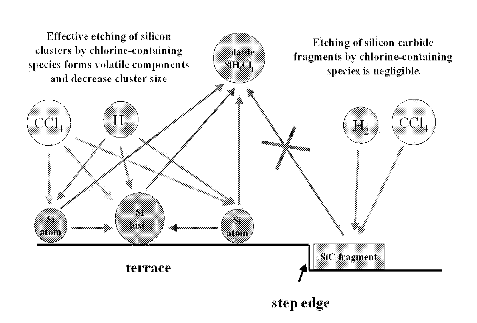
[0018]For example, for a wafer with a 0.2 degree miscut, the terrace width is 721 angstroms, greater than 10 times the terrace width of the off-axis substrates. At these large terrace widths, the supersaturation of the growth species is high, and the probability of 2D nucleation and 3C polytype formation is significantly increased. Additionally, macro-step formation, due to step bunching, can occur. This phenomenon creates terraces with lateral dimensions of microns, further increasing the probability of 2D nucleation. At high growth rates and with a deficiency in the step edges, silicon atoms can form a cluster (before they will encounter a step edge). So, the terraces (regions between steps) can be filled with silicon clusters, which in turn cause 3C—SiC inclusions. Two opposite processes occur here: further cluster growth due to the addition of silicon atoms, migrating on the surface; and cluster evaporation, decreasing the cluster size. It is well-known that some critical size of such clusters exists, and if these clusters grow beyond this critical size, they will introduce regions of cubic SiC in the grown layer. Thus, the introduction of cubic SiC growth is quite likely during the growth on on-axis wafers.
[0020]The addition of chlorine, such as from CCl4, improves the material quality, by eliminating Si clusters and reducing the supersaturation ratio during epitaxial growth, as described below.

Problems solved by technology

Despite the obvious advantages, wide-scale application of SiC in the device industry is currently hindered by difficulties arising in manufacturing of SiC-based structures of the required high quality (and by their high costs).
One item that presently hinders the realization of stable bipolar devices (for example) is stacking faults, which are generated from basal plane dislocations that have propagated from the substrate into the active region of the device during epitaxial growth.
These stacking faults, if present in the active region of the device, result in devices with functional properties that can change unpredictably during operation.
However, if the basal-plane dislocations are efficiently converted into threading edge dislocations, the “killer” stacking faults will not be generated.

Method used


Image

  • METHOD, SYSTEM, AND APPARATUS FOR THE GROWTH OF ON-AXIS SiC AND SIMILAR SEMICONDUCTOR MATERIALS
  • METHOD, SYSTEM, AND APPARATUS FOR THE GROWTH OF ON-AXIS SiC AND SIMILAR SEMICONDUCTOR MATERIALS
  • METHOD, SYSTEM, AND APPARATUS FOR THE GROWTH OF ON-AXIS SiC AND SIMILAR SEMICONDUCTOR MATERIALS

Examples


Embodiment Construction

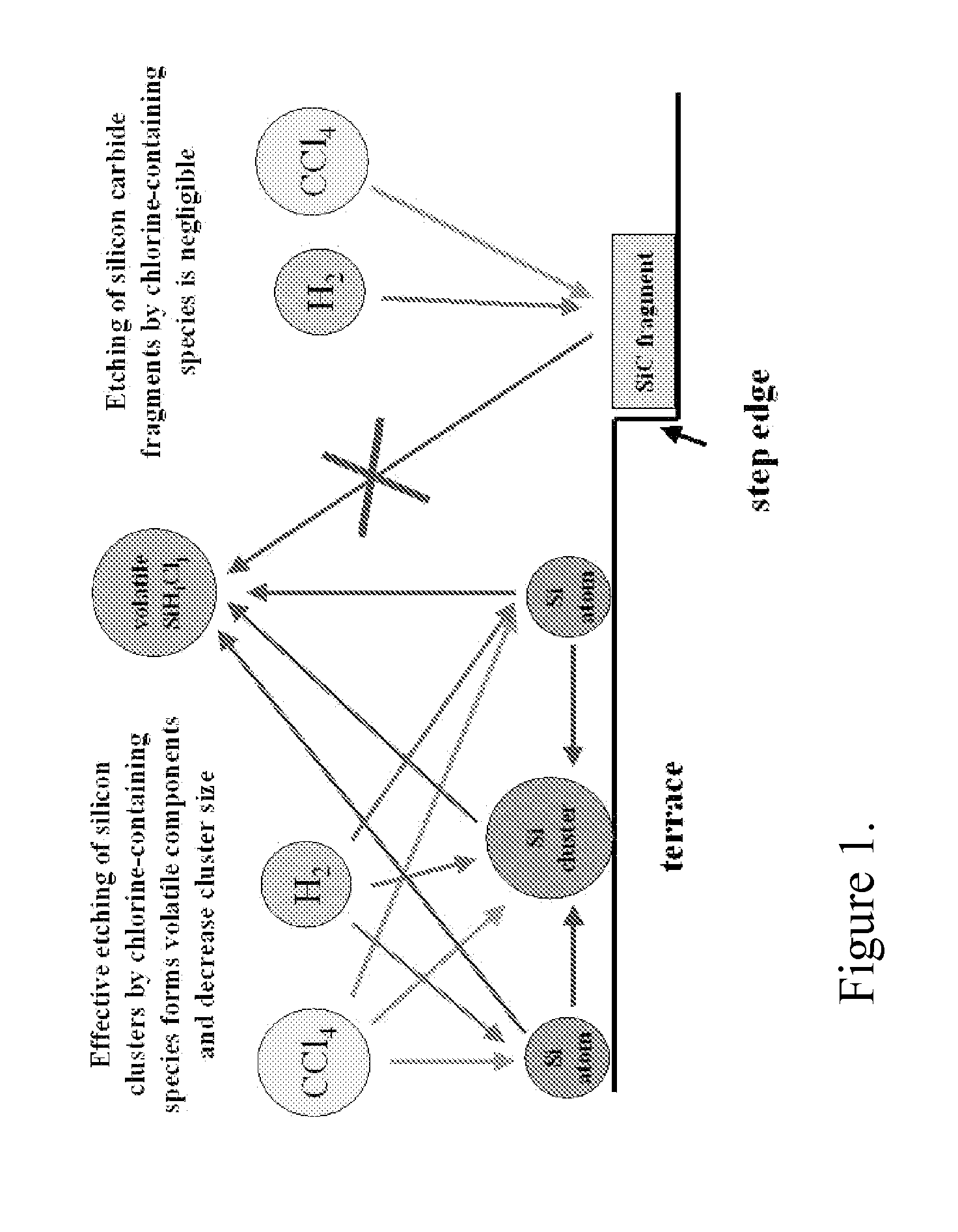
[0026]Chlorine addition provides two mechanisms for promotion of “on-axis” growth. First, chlorine provides an additional removal mechanism for silicon clusters. FIG. 1 illustrates the scheme of such a mechanism. The etching rate for silicon clusters is much higher than that for silicon carbide fragments, formed at the step edges. Effective etching of silicon clusters by chlorine-containing species forms volatile components and decreases average cluster size. So, one can expect that silicon clusters will be maintained below the critical size, for the following silicon-to-carbon and silicon-to-chlorine ratios:

x(int)(Si) / x(int)(C)=0.7−1.3,

x(int)(Si) / x(int)(Cl)=0.03−1,

[0027]where x(int)(Si), x(int)(C), x(int)(Cl) are the numbers of silicon, carbon, and chlorine atoms in the input gas mixture, respectively. As a result, cubic SiC growth will be suppressed on on-axis wafers, while polytype replication will be the dominant growth process. Thus, high quality SiC growth on the on-axis wafer...


PUM

PropertyMeasurementUnit
Angleaaaaaaaaaa
Angleaaaaaaaaaa
Temperatureaaaaaaaaaa

Abstract

A novel approach for the growth of high-quality on-axis epitaxial silicon carbide (SiC) films and boules, using the Chemical Vapor Deposition (CVD) technique, is described here. The method includes a method of substrate preparation, which allows for the growth of “on-axis” SiC films, plus an approach giving the opportunity to grow silicon carbide on singular (a small-angle miscut) substrates, using halogenated carbon-containing precursors (carbon tetrachloride, CCl4, or halogenated hydrocarbons, CHCl3, CH2Cl2, or CH3Cl, or similar compounds or chemicals), or introducing other chlorine-containing species, in the gas phase, in the growth chamber. At gas mixtures greater than the critical amount, small clusters of SiC are etched, before they can become stable nuclei. The presence of chlorine and the formation of gas species allow an increased removal rate of these nuclei, in contrast to the growth without the presence of chlorine. Or, alternatively, the novel precursors introduced in the growth system reduce the effective supersaturation ratio of the Si species in the growth layer. The reduction of the supersaturation ratio reduces or eliminates the 2D (and 3C—SiC) nucleation which would occur due to the large terrace widths present on the on-axis wafers. This allows the growth of Silicon Carbide epitaxial layers on SiC substrates or composite substrates with monocrystalline layers. This can also be applied to the other semiconductors, chemicals, compounds, materials, growth methods, or devices.

Description

RELATED APPLICATIONS[0001]The current application is related to the two co-pending application Ser. Nos. 11 / 626,388 and 11 / 626,387, both filed Jan. 24, 2007, both owned by one of the assignees of the current application (Widetronix Inc., Ithaca, N.Y.), and both have the same inventors as the ones in the current case: Yuri Makarov and Michael Spencer. The entire contents of which are incorporated herein, by reference.FIELD OF THE INVENTION[0002]The disclosure relates to the semiconductor materials. More specifically, the disclosure relates to the epitaxial growth of silicon carbide and similar materials, by chemical vapor deposition and other growth methods.BACKGROUND OF THE INVENTION[0003]Silicon Carbide[0004]The superior properties of silicon carbide, as compared with silicon, make it a perspective material for high power and high-temperature electronics (e.g. high-power transistors, thyristors, devices with P-type and N-type conductivity layers (e.g. diodes), and rectifiers). Due ...

Claims


Application Information

Patent Timeline
IPC IPC(8): C23C16/458
CPCC30B29/36C30B25/18
Inventor MAKAROV, YURISPENCER, MICHAEL
Owner WIDETRONIX
Learn More