

Semiconductor optical modulator
- Summary
- Abstract
- Description
- Claims
- Application Information
AI Technical Summary
Benefits of technology
Problems solved by technology
Method used
Image

Examples
first embodiment
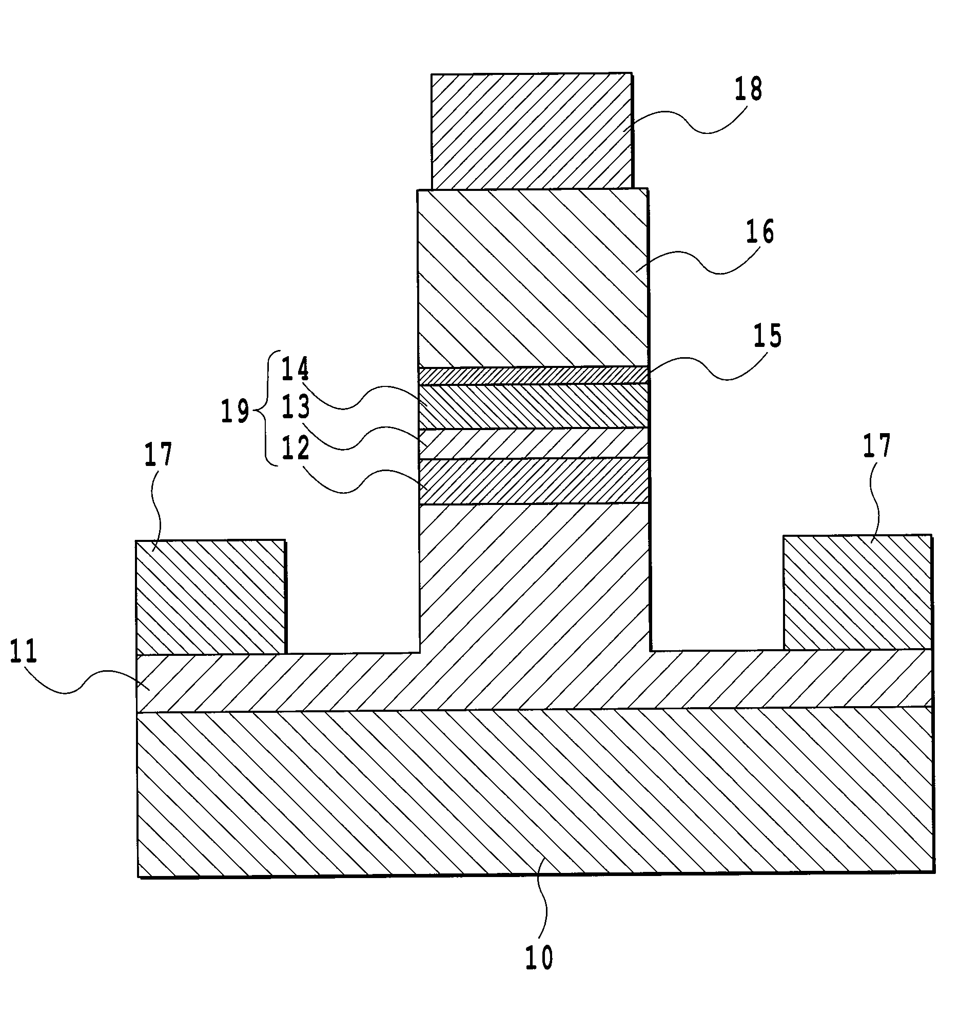
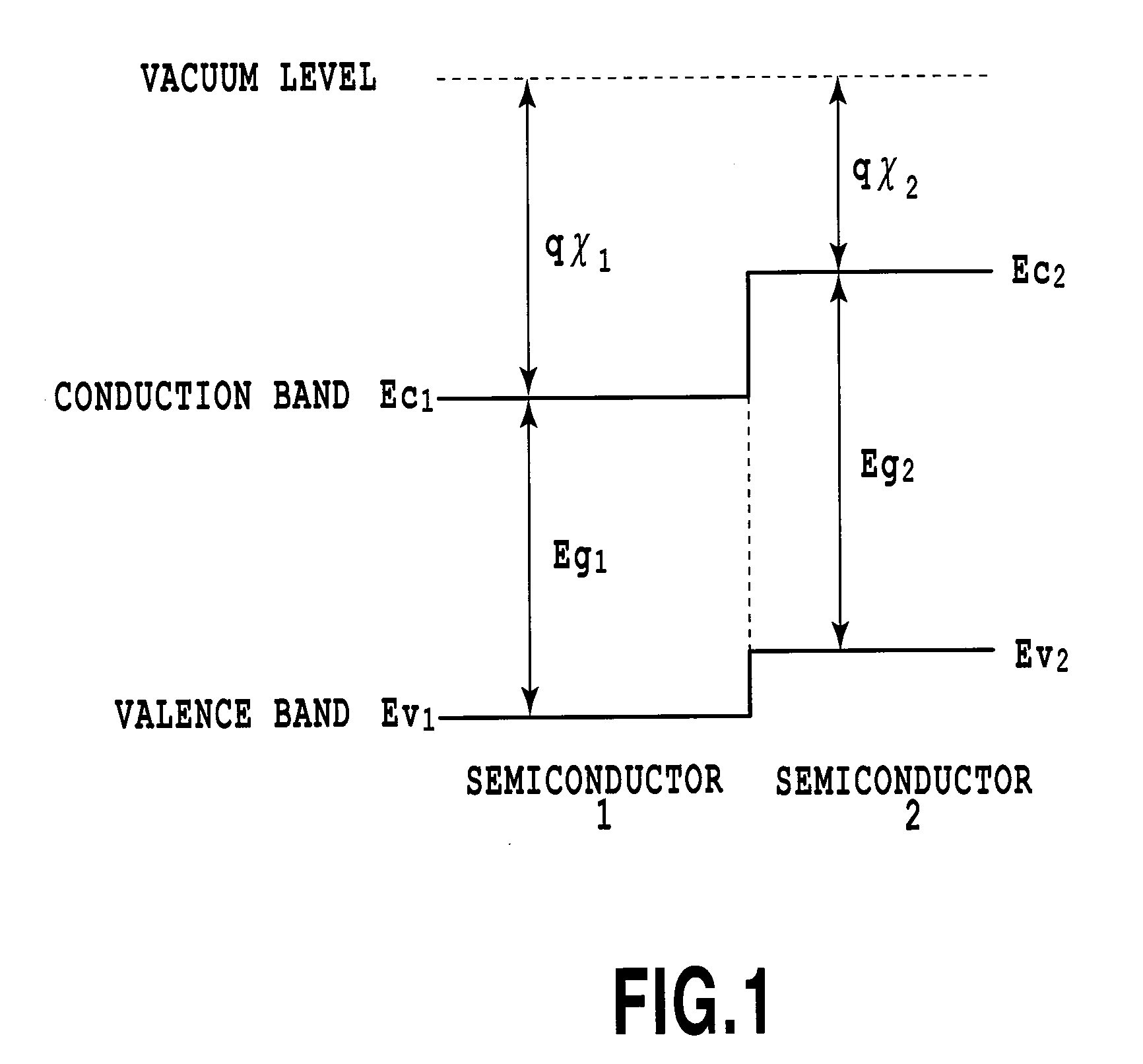
[0064]In the semiconductor optical modulator of the present embodiment, a first n-type semiconductor clad layer, a semiconductor optical waveguide layer having an electronic-optic effect, a semiconductor clad layer, and a second n-type semiconductor clad layer are sequentially grown. Such a layer structure has an n-i-n structure, and the present embodiment is designed so that the semiconductor clad layer and the second n-type semiconductor clad layer would have a heterojunction and an electron affinity of the semiconductor clad layer would become smaller than an electron affinity of the second n-type semiconductor clad layer. By doing so, the semiconductor clad layer becomes a potential barrier for electrons of the second n-type semiconductor clad layer. With this, it is possible to achieve an optical modulator performing a more stable operation and having an excellent voltage-current characteristic (high breakdown voltage, and low leak current) to an electric field, without losing ...
example
[0086]In an example to be described below, InP was used for the first and second n-type semiconductor clad layers. Ap-type InAlAs layer (p-InAlAs layer 16) was used for the semiconductor clad layer functioning as a potential barrier for electrons, and a layer thickness was set to 0.05 μm and doping density was set to 1×1018 cm-3. In addition, a total thickness of the semiconductor optical waveguide 19, that is, the non-dope layer was set to 0.9 μm, and a width of the semiconductor optical waveguide layer 19 was set to 1.6 μm.
[0087]FIGS. 4 to 6 show the characteristic of the Mach-Zehnder modulator manufactured by using the above parameters. FIG. 4 is a graph showing a voltage-current characteristic in a case where a negative voltage (inverse bias) is applied to the electrode 18 between the electrodes 17 and 18. As is clear from FIG. 4, it is seen that the sufficient voltage-current characteristic of 15V or more is shown.
[0088]In addition, FIG. 5 shows an E / E high-frequency response c...
second embodiment
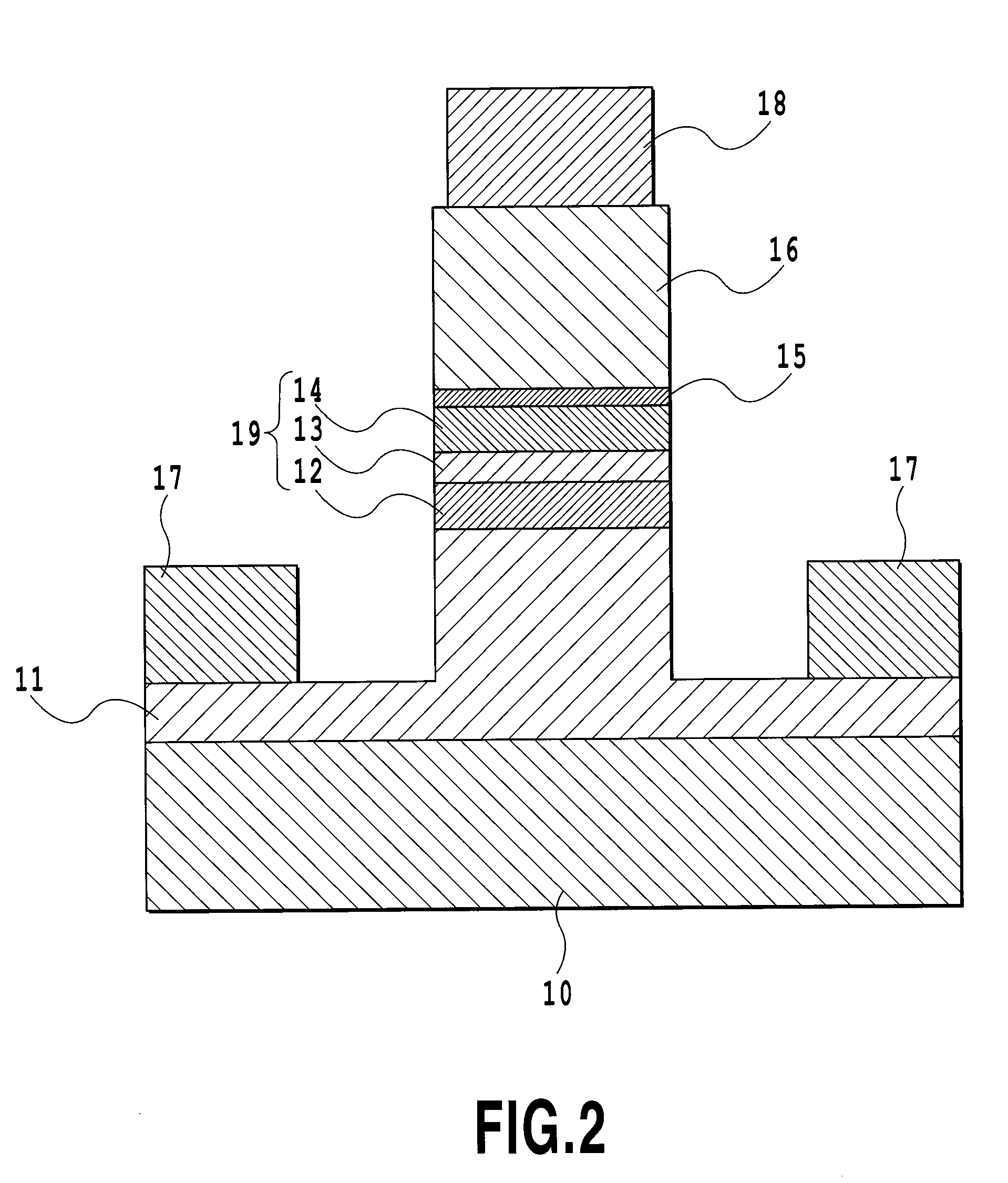
[0090]FIG. 7 is a diagram showing a band diagram of a waveguide structure of the semiconductor optical modulator according to the present embodiment.
[0091]A basic structure of the semiconductor optical modulator according to the present embodiment is the same as that of the first embodiment, and the description thereof will be omitted. A point of the present embodiment different from that of the first embodiment is that a third n-type semiconductor clad layer 20 having a potential energy for holes, which is smaller than that of an n-InP clad layer 16 being a second n-type semiconductor clad layer, is inserted between the n-InP clad layer 16 being the second n-type semiconductor clad layer and a p-InAlAs layer 15 being a potential barrier layer. This third n-type semiconductor clad layer 20 can be formed by properly setting compositions by, for example, an InGaAsP layer, an InGaAlAs layer, and the like.
[0092]With this, the holes in a semiconductor core layer 13, which are slightly ca...
PUM
 Abstract
Description
Claims
Application Information