Cmp apparatus and method of polishing wafer using cmp

a technology of chemical mechanical polishing and polishing equipment, which is applied in the direction of lapping machines, manufacturing tools, abrasive surface conditioning devices, etc., can solve the problems of low yield and other problems, inability to transfer precise patterns, and inability to fix the focus during exposure, so as to improve the effect of outpu

Inactive Publication Date: 2009-02-05
PS4 LUXCO SARL
View PDF4 Cites 33 Cited by
  • Summary
  • Abstract
  • Description
  • Claims
  • Application Information

AI Technical Summary

Benefits of technology

[0012]In this way, according to the present invention, the timing for switching the polishing conditions in metal-based CMP can be precisely measured, and throughput improvement and erosion prevention can be assured because a threshold value of an eddy current sensor can be corrected in accordance with the thickness of the polishing pad.

Problems solved by technology

When there are convexities and concavities or steps in the substrate when a film is formed, the thickness of the film formed on the substrate will be thin in parts and step coverage will worsen, causing lower yield and other problems.
Also, problems occur in that focus during exposure is not fixed and precise patterns cannot be transferred because convexities and concavities appear in upper layers due to the effect of the lower patterned layers.
However, when tungsten (W), copper (Cu), titanium nitride (TiN) or another metal film is polished at high speed, there is a problem in that erosion increases.
Therefore, there is a problem in that CMP throughput is reduced.
Since the remaining film becomes thin when the polishing pad is thin, quality degradation is liable to occur due to erosion and the like.

Method used


Image

  • Cmp apparatus and method of polishing wafer using cmp
  • Cmp apparatus and method of polishing wafer using cmp
  • Cmp apparatus and method of polishing wafer using cmp

Examples


Embodiment Construction

[0017]Preferred embodiments of the present invention will be described hereinafter with reference to the accompanying diagrams.

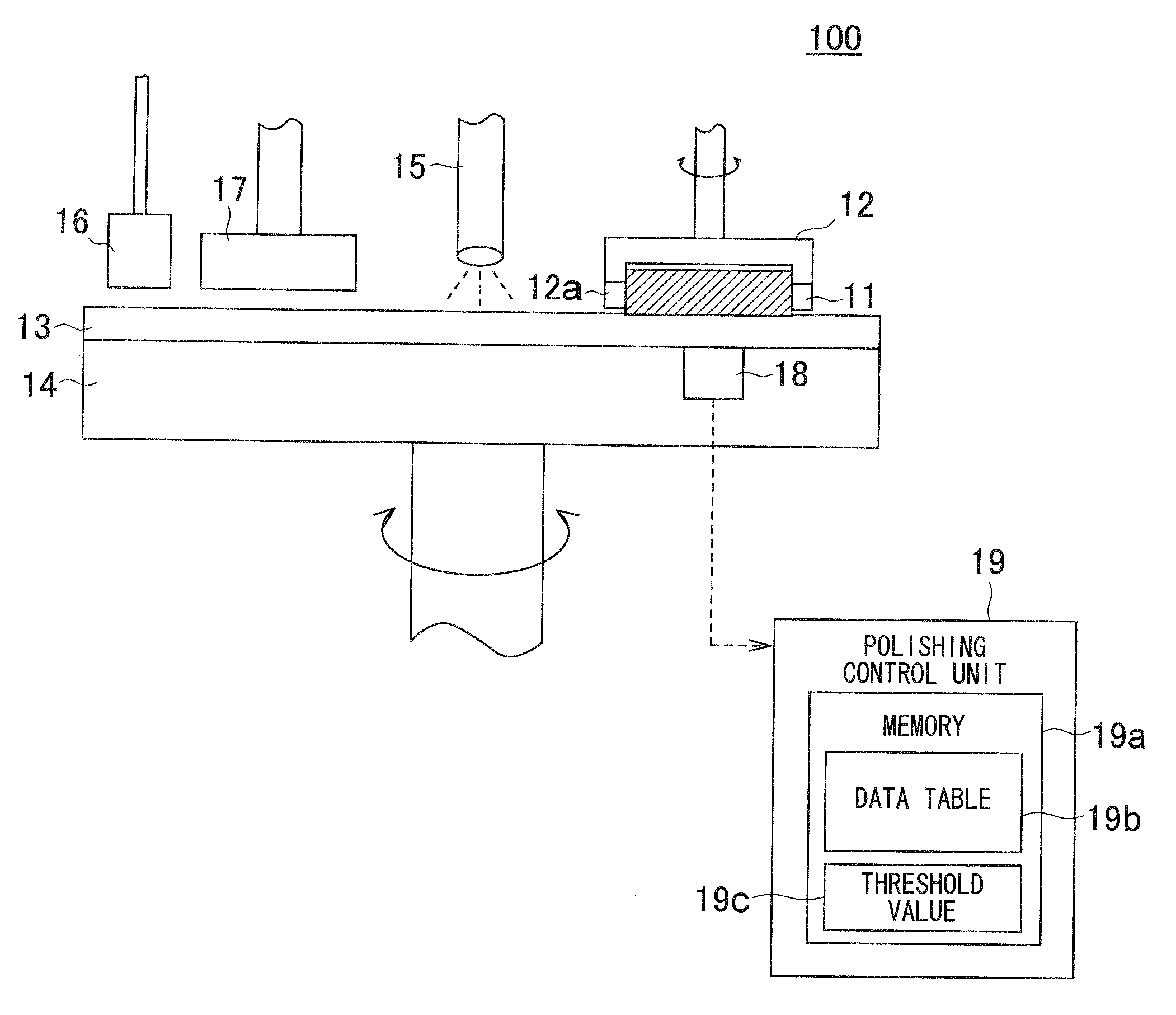
[0018]FIG. 1 is a schematic view showing a configuration of a CMP apparatus according to a preferred embodiment of the present invention.

[0019]As shown in FIG. 1, the CMP apparatus 100 is provided with a polishing head 12 for holding a wafer 11, a rotary surface plate 14 on which a polishing pad 13 is mounted, a slurry supply unit 15 for supplying a slurry that contains silica (SiO2) microparticles or another abrasive, a pad probe 16 for measuring the state of a polishing pad 13, a dresser 17 for dressing the polishing pad 13, an eddy current sensor 18 for measuring the thickness of a tungsten film, which is the metal film being polished on the wafer 11, and a polishing control unit 19 that controls these components.

[0020]The polishing head 12 is provided with a spindle mechanism for rotating the wafer 11, and a pressing mechanism for pressing the wafer 11 a...


PUM

PropertyMeasurementUnit
thicknessaaaaaaaaaa
thicknessaaaaaaaaaa
thicknessaaaaaaaaaa

Abstract

A CMP apparatus is provided with a polishing pad, a film thickness sensor for measuring a thickness of a film being polished on a wafer via the polishing pad, a polishing pad thickness measuring unit for measuring the thickness of the polishing pad, a dresser for dressing the polishing pad, and a polishing control unit for switching polishing conditions in response to a fact that an output value from the film thickness sensor has exceeded a threshold value. The polishing control unit has a memory unit for storing a threshold value corresponding to the thickness of the polishing pad after dressing when the polishing pad is dressed.

Description

TECHNICAL FIELD[0001]The present invention relates to a CMP (chemical mechanical polishing) apparatus and a method of polishing a semiconductor wafer using the CMP, and more particularly relates to a method for detecting timing for switching polishing speed.BACKGROUND OF THE INVENTION[0002]CMP is an important technique in manufacturing semiconductor devices. Semiconductor integrated circuit chips are manufactured by forming conductive layers, insulating layers, or other thin film layers in a prescribed order on a wafer, patterning the layers depending on need by photolithography and etching, and cutting and separating each chip on the wafer after forming all layers. When there are convexities and concavities or steps in the substrate when a film is formed, the thickness of the film formed on the substrate will be thin in parts and step coverage will worsen, causing lower yield and other problems. Also, problems occur in that focus during exposure is not fixed and precise patterns ca...

Claims


Application Information

Patent Timeline
Patent Type & Authority Applications(United States)
IPC IPC(8): B24B49/02B24B29/00B24B49/04B24B49/10B24B37/04H01L21/304
CPCB24B37/013B24B53/017B24B49/105
Inventor MATSUZAKI, TORU
Owner PS4 LUXCO SARL
Why Eureka
Try Eureka