Process Of Making An Optical Lens

Inactive Publication Date: 2009-04-23
PANASONIC CORP
View PDF3 Cites 3 Cited by
  • Summary
  • Abstract
  • Description
  • Claims
  • Application Information

AI Technical Summary

Benefits of technology

[0009]In one version of the present invention, the anode is formed partially on the bottom surface of the substrate to give one or more circular anode pattern which defines the predetermined distribution of the electric field intensity, and is responsible for realizing the curved surface having a concave profile at a portion opposed to the circular anode pattern. Therefore, it is easy to fabricate a concave lens of desired radius of curvature by suitably designing the anode pattern.
[0010]In anoth

Problems solved by technology

However, it is found practically difficult to give a thick profile with a smoothly curved surface as is required in fabricating the optical lens, since the oxidized portions act as a dielectric barrier blocking an anodizing current through the substrate to inhibit the growth of the oxidized portions in the thickness of the substrate.
In this sense, the above prior art is found not to be available for fabrication of the optical lens with sufficient thickness.
With this limitation, the process cannot be not adapted to fabricate optical lens having non-uniform radius of curvature or sophisticated surface profile.
However, bubbles appearing in the initial stage are difficult to escape out through the tiny opening and are likely to remain in the porous zones, which inhibits the entry of the electrolyte solution in the substrate and therefore impedes further development of the porous zone.
With this result, the porous zones could not be controlled to give an int

Method used


Image

  • Process Of Making An Optical Lens
  • Process Of Making An Optical Lens
  • Process Of Making An Optical Lens

Examples


example

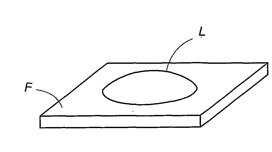
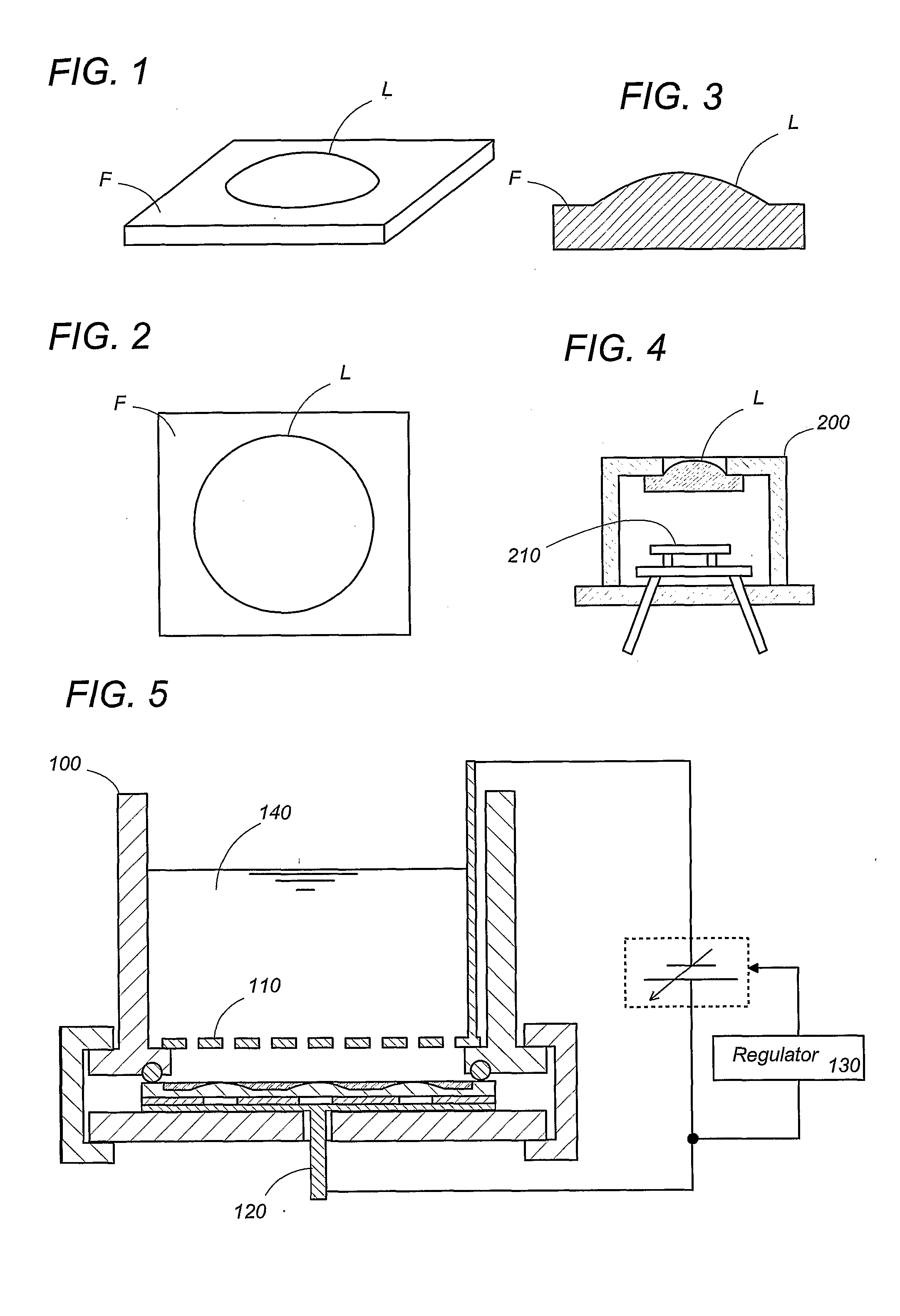
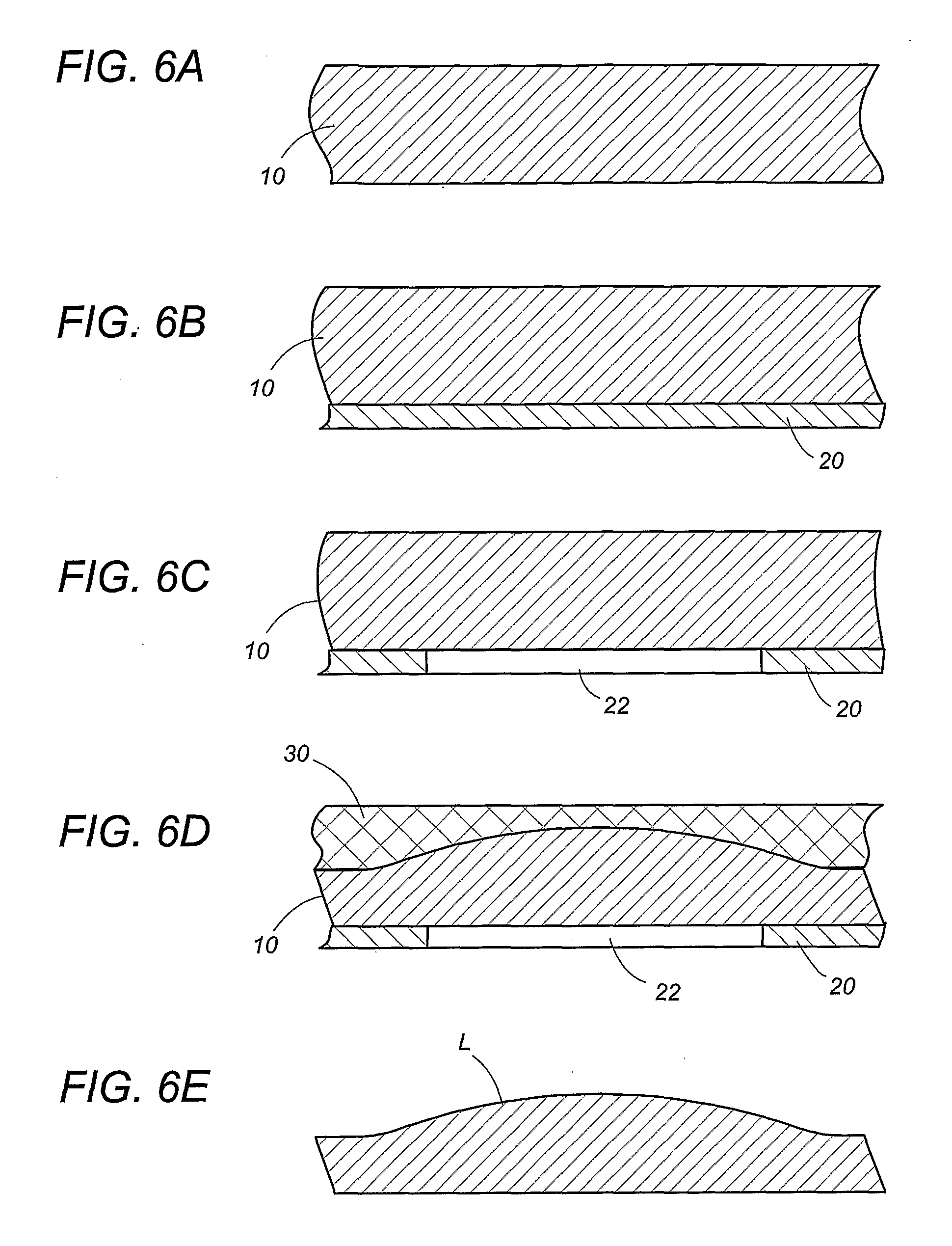
[0047]A 100 mm diameter p-type Si substrate 10 of 0.5 mm thick and 80 Ω·cm resistivity was formed on its bottom surface with a 1 μm thick aluminum conductive layer 20 by spattering. After sintering the conductive layer 20 at 420° C. for 20 minutes, the layer 20 was masked by photolithography with a resist pattern having a plurality of windows of 2 mm diameters. Then, the unmasked portion of the conductive layer 20 was etched out to form a plurality of 2 mm diameter openings in the conductive layer, as shown in FIG. 8. After being removed of the resist pattern, the substrate 10 was placed in the anodizing apparatus of FIG. 5 containing the electrolytic solution comprised of an 1:1 ratio mixture of a 50% aqueous solution of hydrogen fluoride (HF) and ethanol. Then, the substrate was anodized at current density of 30 mA / cm2 for 3 hours. The resulting porous layer 30 was found to have a 0.3 mm thick at the portion corresponding to the conductive layer 20 and to have a decreasing thickne...

second embodiment

[0049]FIGS. 11 and 12 illustrate the process of fabricating a plano-concave lens L in accordance with the second embodiment of the present invention. In the present invention, the semiconductor substrate 10 is formed on its bottom surface with an anode pattern composed of a plurality of circular anodes 20 in a pattern analogous to that shown in FIG. 8. For simplicity, only single anode 20 is shown in FIGS. 12A and 12B. Each anode 20 is responsible for forming a concave profile in the opposing top surface of the substrate 10 by anodization and by removal of the resulting porous layers 30 in the like manner as discussed with reference to the first embodiment. That is, during the anodizing process, the porous layer 30 develops in the top surface at a portion opposed to each anode 20 to have a depth which is greater towards the center of each electrode 20 than at the periphery thereof, as shown in FIG. 12B. Then, the porous layer 30 and the anode 20 are etched out to uncover the concave...

third embodiment

[0050]FIG. 13 illustrates the process of fabricating a double-convex lens L in accordance with the third embodiment of the present invention which is similar to the first embodiment except for inclusion of additional anodization process. Firstly, the substrate 10 is formed in its top surface with the convex profile through the steps as described in the first embodiment and as shown in FIGS. 13A to 13D. Then, an additional conductive layer 24 with a plurality of additional circular openings 26 is deposited on the top surface with each of the additional circular openings 26 being disposed in concentric with the already formed convex profile as shown in FIG. 13E, in which only one additional circular opening 26 is shown for simplicity. Subsequently, the substrate 10 is anodized to develop an additional porous layer 34 in the bottom surface of the substrate 10, as shown in FIG. 13F. The additional porous layer 34 is etched out together with the additional conductive layer 24 to obtain t...


PUM

PropertyMeasurementUnit
Dielectric polarization enthalpyaaaaaaaaaa
Electrical conductivityaaaaaaaaaa
Electrical resistanceaaaaaaaaaa

Abstract

A semiconductor substrate is anodized to be shaped into an optical lens. Prior to being anodized, the substrate is finished with an anode pattern on its bottom surface so as to be consolidated into a unitary structure in which the anode pattern is precisely reproduced on the substrate. The anodization utilizes an electrolytic solution which etches out oxidized portion as soon as it is formed as a result of the anodization, to thereby develop a porous layer in a pattern in match with the anode pattern. The anode pattern brings about an in-plane distribution of varying electric field intensity by which the porous layer develops into a shape complementary to a desired lens profile. Upon completion of the anodization, the semiconductor substrate is shaped into the lens by etching out the porous layer and the anode pattern from the substrate.

Description

TECHNICAL FIELD[0001]The present invention is directed to a process for fabricating an optical lens from a body of semiconductor substrate.BACKGROUND ART[0002]One prior art is disclosed in Japanese patent publication No. 55-13960 which is directed to a process of making a micro structure in the surface of a semiconductor substrate by anodization. The anodization is used for oxidizing the top surface of the substrate in an electrolyte solution. The oxidizing proceeds selectively in the top surface in a pattern corresponding to an arrangement of an anode. The anode is formed separately from the substrate and is held in contact with the bottom surface of the substrate, leaving oxidized portions partially in the top surface of the substrate. Thereafter, the oxidized portions are removed to leave a convex in the top surface of the substrate. This technique is sufficient for forming a relatively thin profile or surface irregularity with a small depth. However, it is found practically diff...

Claims


Application Information

Patent Timeline
IPC IPC(8): C25D5/02C25F3/12
CPCB29D11/00019B29D11/00298G02B3/02G02B3/0031G02B3/0056G02B3/0006G02B3/0012
Inventor HONDA, YOSHIAKINISHIKAWA, TAKAYUKI
Owner PANASONIC CORP
Why Eureka
Try Eureka