Semiconductor device and method for manufacturing the same, dry-etching process, method for making electrical connections, and etching apparatus

a technology of semiconductor devices and resist patterns, applied in semiconductor devices, semiconductor/solid-state device details, electrical devices, etc., can solve the problems of reducing the manufacturing yield of semiconductor devices, achieve accurate etching of underlying materials, transfer resist patterns accurately onto underlying materials, and good yield

Inactive Publication Date: 2009-04-23
PHILTECH
View PDF5 Cites 8 Cited by
  • Summary
  • Abstract
  • Description
  • Claims
  • Application Information

AI Technical Summary

Benefits of technology

[0022]As has been discussed above, in the conventional method for the production of semiconductor devices, ArF-photolithography should be employed as a means for producing a semiconductor device containing a fine pattern having a width on the order of not more than 130 nm, and in particular, not more than 100 nm. Accordingly, a problem arises such that the manufacture yield of semiconductor devices is reduced since the rate of striations with respect to the pattern size of, for instance, the gate length, the electrical connection width or the diameter of contact holes increases.
[0023]It is accordingly an aspect of the present invention to provide a semiconductor device and a method for the manufacture thereof so designed that etching can be performed without causing any damage of a less-durable resist mask for ArF-photolithography even if the resist carries fine patterns having a size of not more than 130 nm and is formed using ArF-photolithography. This can likewise permit the solution of the foregoing problems associated with the conventional method and can thus control the generation of striation and improve the production yield of the semiconductor device.
[0024]It is another aspect of the present invention to provide a dry-etching process which permits etching without damaging a less-durable resist and a method for making electrical connections using this dry-etching process.

Problems solved by technology

Accordingly, a problem arises such that the manufacture yield of semiconductor devices is reduced since the rate of striations with respect to the pattern size of, for instance, the gate length, the electrical connection width or the diameter of contact holes increases.

Method used


Image

  • Semiconductor device and method for manufacturing the same, dry-etching process, method for making electrical connections, and etching apparatus
  • Semiconductor device and method for manufacturing the same, dry-etching process, method for making electrical connections, and etching apparatus
  • Semiconductor device and method for manufacturing the same, dry-etching process, method for making electrical connections, and etching apparatus

Examples


example 1

[0096]In the present invention, in this Example, a dielectric film was prepared by growing (or depositing) an oxide film (TEOS-SiO2) on a silicon substrate (wafer) to a thickness of 300 nm using TEOS gas by plasma CVD.

[0097]An anti-reflection film and then a resist film for ArF-photolithography were successively coated such that the dielectric film was covered with these films. An electrical connection pattern containing grooves each having a width of 100 nm was formed thereon while using ArF-photolithography. Thereafter, the dielectric film covered with the resist film carrying this electrical connection pattern was subjected to dry-etching within a plasma atmosphere.

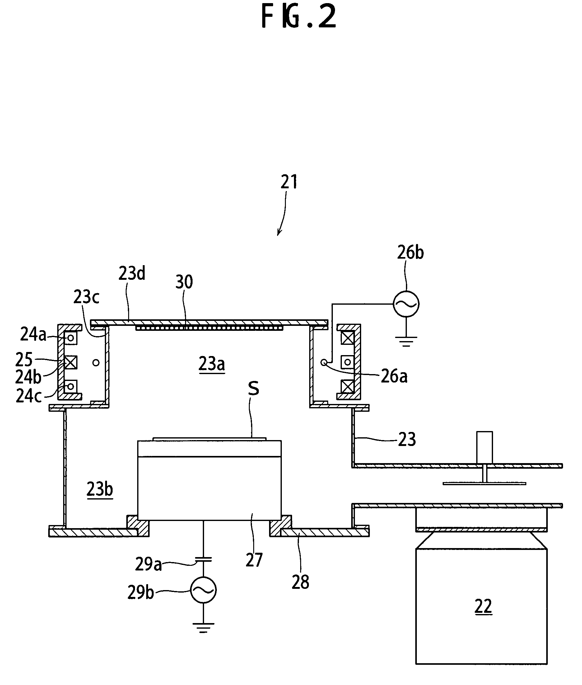
[0098]During etching, the dielectric film was etched by introducing Ar and C3F7I as an etching gas into the vacuum chamber 23 of the etching apparatus 21 at a pressure of 2.67 Pa to form grooves each having a width of 100 nm. The resist was then removed. At this stage, the flow rates of Ar, C3F7I gas and oxygen gas wer...

example 2

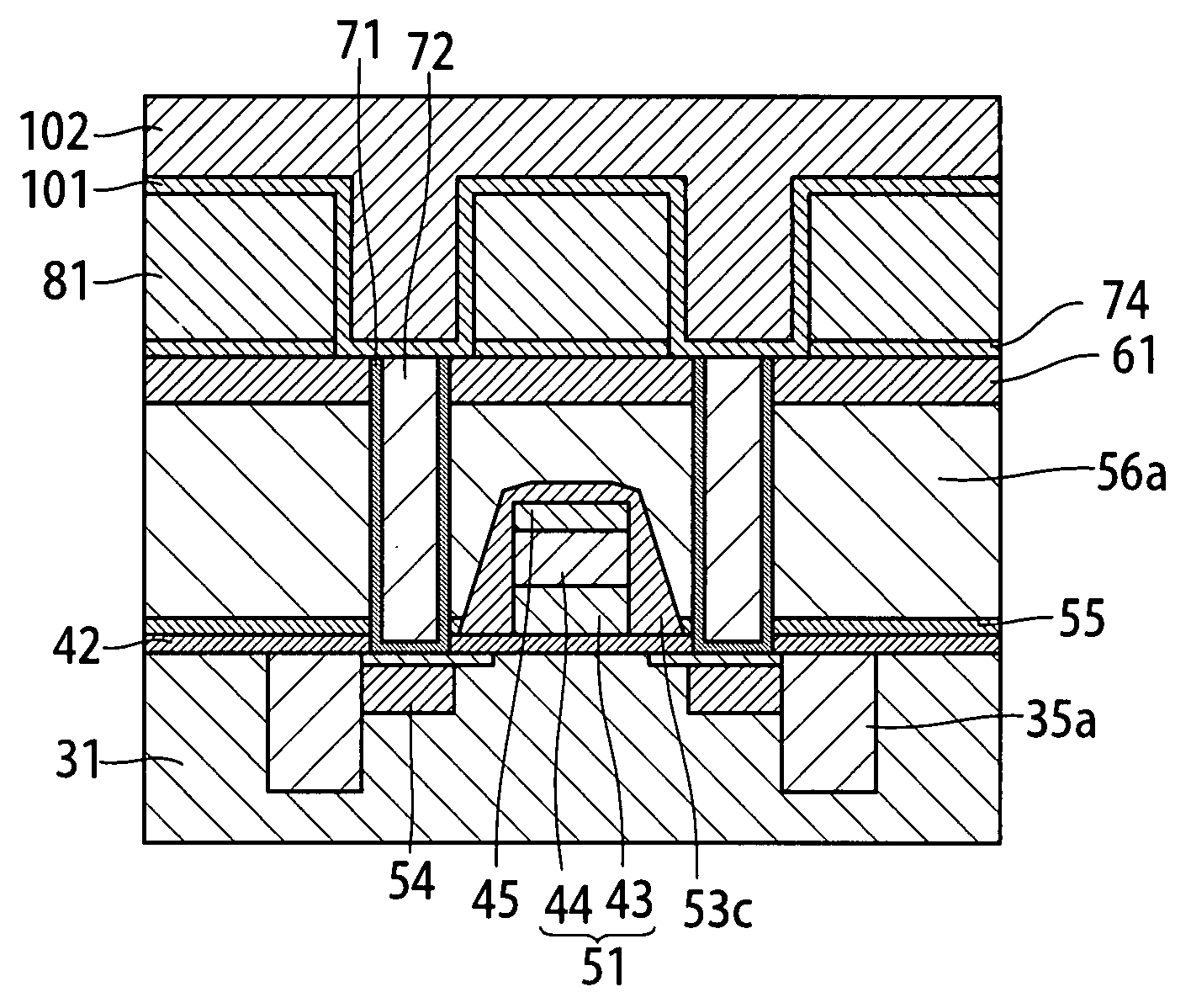
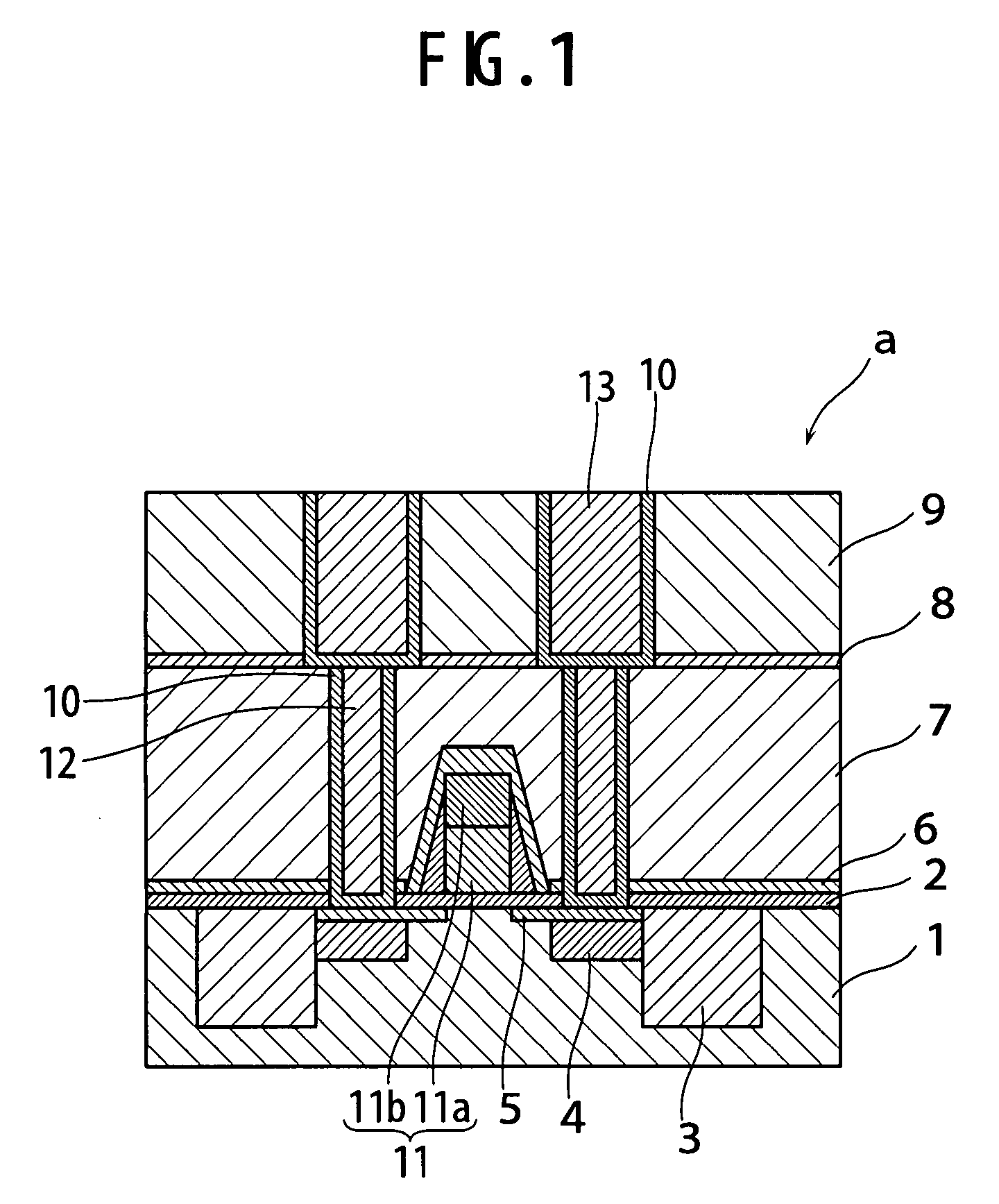
[0102]Example 2 is given for the explanation of a method for forming a Cu electrical connection pattern of a semiconductor device according to the Cu-damascene technique. The following description of the basic or essential parts of a process is for forming only one layer, but two or more electrical connection layers can likewise be formed by repeating the following procedures or adding some modifications thereto (see, for instance, FIGS. 12(a) to (c)).

[0103](1) First, a TEOS-SiO2 film 122a was formed on an Si substrate 121 in a thickness of 250 nm at a temperature of 400° C. using plasma CVD. A cap-SiN film 122b was grown thereon to a thickness of 50 nm.

[0104](2) An interlayer dielectric film 122c of TEOS-SiO2 on which Cu-electrical connections would be formed was formed on the SiN film 122b in a thickness of 200 nm at a temperature of 400° C. using plasma CVD. A plasma silicon nitride film (p-SiN) 122d as a CMP stopper was deposited on the dielectric film 122c to a thickness of 30 ...

example 3

[0129]Example 3 is given explaining the principal steps for accurately producing the gates included in the semiconductor device a according to the present invention. In this respect, FIGS. 13(a) to (c) and 13(a′) to (c′) schematically show respective cross-sectional views and top plan views of the semiconductor device obtained after the completion of these principal steps, respectively. In this connection, any known method can be used as, for instance, a dielectric isolation step of a transistor prior to the production of gates; a step for producing a gate-insulating film; a side wall-forming step after the etching of the gate-forming material; and a source and drain-diffusion step. Therefore, the description of these steps are herein omitted.

[0130](1) A gate oxide film 132 was grown on a silicon (Si) wafer 131 to a predetermined thickness and a doped amorphous Si (a-Si) film 133a was then formed at 500° C. using known CVD to a thickness of 200 nm.

[0131](2) A tungsten (W) film 133b ...


PUM

PropertyMeasurementUnit
widthaaaaaaaaaa
relative dielectric constantaaaaaaaaaa

Abstract

A method for manufacturing a semiconductor device comprises dry-etching a thin film using a resist mask carrying patterns in which at least one of the width of each pattern and the space between neighboring two patterns ranges from 32 to 130 nm using a halogenated carbon-containing compound gas with the halogen being at least two members selected from the group consisting of F, I and Br. The ratio of at least one of I and Br is not more than 26% of the total amount of the halogen atoms as expressed in terms of the atomic compositional ratio to transfer the patterns onto the thin film. Such etching of a thin film avoids causing damage to the resist mask used. The resulting thin film carrying the transferred patterns is used as a mask for subjecting the underlying material to dry-etching.

Description

BACKGROUND OF THE INVENTION[0001]1. Field of the Invention[0002]The present invention relates to a semiconductor device and a method for manufacturing the same and, in particular, to a semiconductor device and a method for manufacturing the same, wherein etching is carried out without any accompanying damage to a less-durable resist used during ArF-photolithography and, in turn, a problem is solved concerning Line Edge Roughness (LER; also referred to as “striation”) permitting the formation of fine patterns of not more than 130 nm while ensuring a high degree of accuracy. The present invention likewise relates to a dry-etching process which permits etching without any accompanying damage of a less-durable resist used during ArF-photolithography as well as a method for making electrical connections by making use of the dry-etching process.[0003]2. Description of the Related Art[0004]Recently, the structural details of semiconductor devices have gradually become finer and finer and t...

Claims


Application Information

Patent Timeline
Patent Type & Authority Applications(United States)
IPC IPC(8): H01L21/461H01L29/10
CPCH01L21/28061H01L21/31116H01L29/7833H01L29/6659H01L21/76802
Inventor HAYASHI, TOSHIOMORIKAWA, YASUHIROISHIKAWA, MICHIOFURUMURA, YUJIMURA, NAOMI
Owner PHILTECH
Why Eureka
Try Eureka