Method for Fine Processing of Substrate, Method for Fabrication of Substrate, and Light Emitting Device
- Summary
- Abstract
- Description
- Claims
- Application Information
AI Technical Summary
Benefits of technology
Problems solved by technology
Method used
Image

Examples
example 1
[0077]Formation of Structure with Circular-Hole Arrangement on GaN Layer
(Formation of Single Particle Layer)
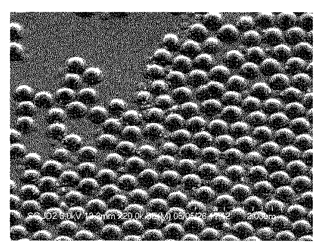
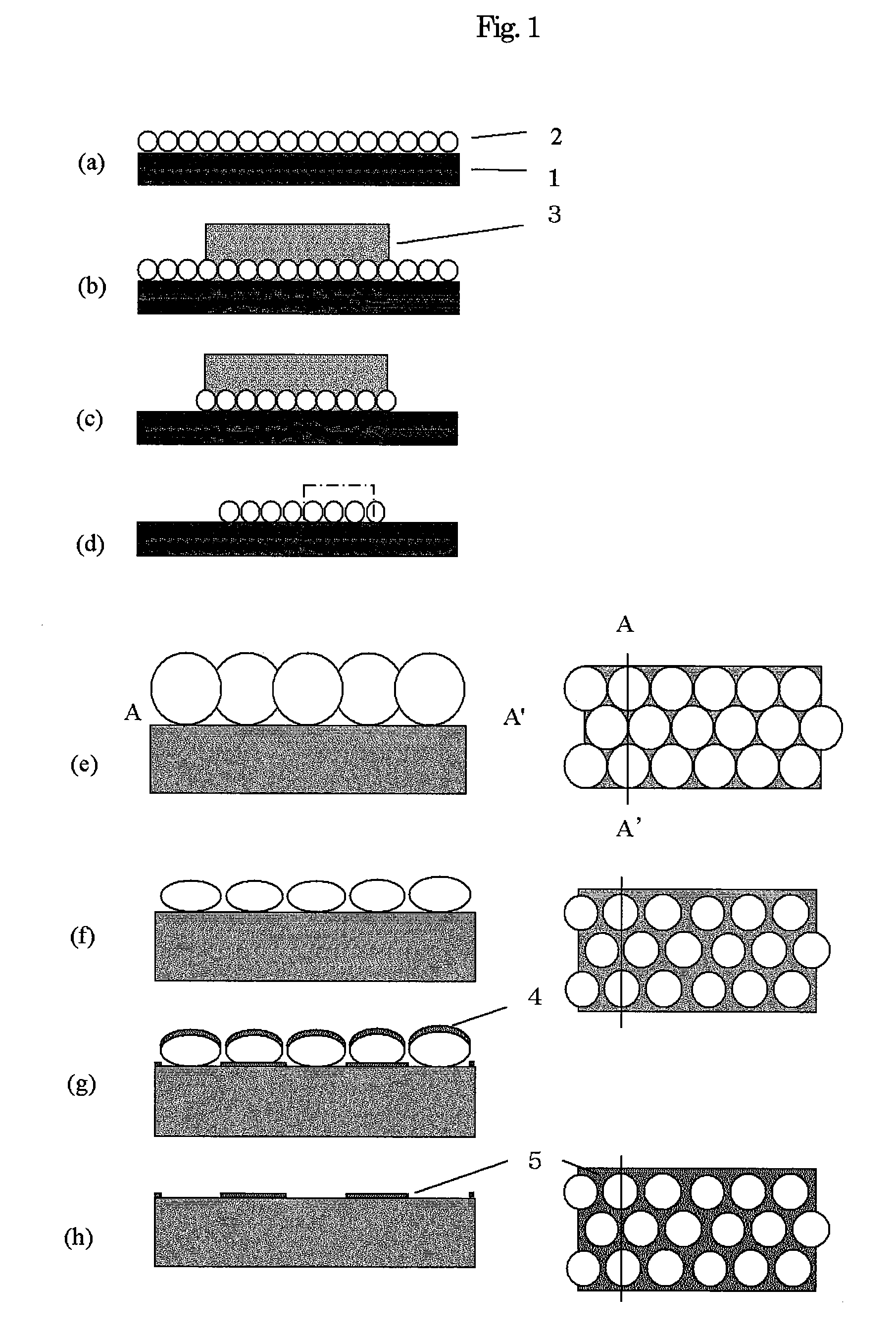
[0078]As an inorganic particle, a silica particle contained in a colloidal silica slurry (product name: PM-4540™ manufactured by Nissan Chemical Industries, Ltd., a first particle diameter: 450 nm, a particle concentration: 40% by weight) was used. A GaN layer was crystal-grown on a sapphire substrate by MOCVD. With the obtained substrate loaded on a spinner, the colloidal silica slurry diluted to 25% by weight was applied on the GaN layer and was spin-dried. A SEM picture of the substrate surface was shown in FIG. 10. A silica single particle layer was formed on the GaN layer. In addition, a two-dimensional closest packing structure was partially formed.
[0079]A pattern was formed on the substrate by normal photolithography using a photo-resist. By processing a portion which is not covered with the photo-resist with buffered hydrofluoric acid, the silica particle in the portio...
example 2
[0087]Formation of Structure with Circular-Hole Arrangement on Sapphire
[0088]By performing the same operations as in (Formation of Single Particle Layer), (First Etching), (Formation of Mask), and (Second Etching) in Example 1 except for the use of a C-face sapphire substrate as a substrate, the structure with the circular-hole arrangement was formed on the sapphire substrate.
[0089]The etch rate for sapphire was almost 0. The selectivity (silica / sapphire) in the first etching was high. The selectivity (Ni mask / sapphire) in the second etching was 5.
example 3
[0090]Formation of Structure with Circular-Hole Arrangement on ITO (an Ohmic p-Electrode of a Light Emitting Diode)
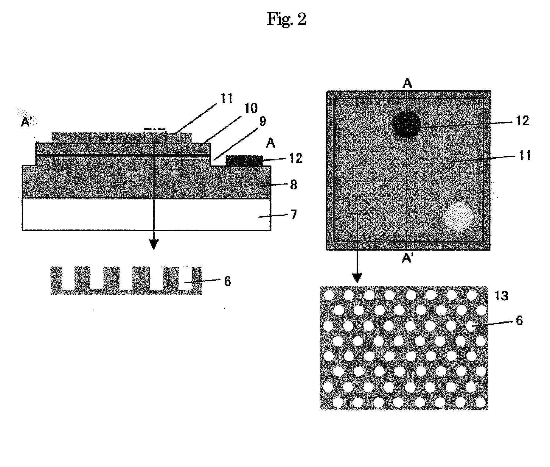
[0091]By forming, on the sapphire, a light emitting device structure composed of the GaN-based semiconductor layer by MOCVD, then an ITO thin film with a thickness of 150 nm in accordance with a facing target sputtering method by performing etching to expose an n-layer, and an ohmic p-electrode pattern by photolithography, a multi-layered substrate was obtained.
[0092]By performing the same operations as in (Formation of Single Particle Layer), (First Etching), (Formation of Mask), and (Second Etching) in Example 1 except for the use of the multi-layered substrate as a substrate, the structure with the circular-hole arrangement was formed on the ITO. Next, by removing the Ni mask with buffered hydrofluoric acid and forming an Al ohmic n-electrode on the n-layer exposed portion, the light emitting device was obtained.
[0093]The etch rate for ITO in the first etching was al...
PUM
 Abstract
Description
Claims
Application Information
 - R&D
- Intellectual Property
- Life Sciences
- Materials
- Tech Scout
- Unparalleled Data Quality
- Higher Quality Content
- 60% Fewer Hallucinations
Browse by: Latest US Patents, China's latest patents, Technical Efficacy Thesaurus, Application Domain, Technology Topic, Popular Technical Reports.
© 2025 PatSnap. All rights reserved.Legal|Privacy policy|Modern Slavery Act Transparency Statement|Sitemap|About US| Contact US: help@patsnap.com