Field effect transistor containing a wide band gap semiconductor material in a drain

Inactive Publication Date: 2009-05-14
GLOBALFOUNDRIES INC
View PDF15 Cites 81 Cited by
  • Summary
  • Abstract
  • Description
  • Claims
  • Application Information

AI Technical Summary

Benefits of technology

[0009]The present invention addresses the needs described above by providing a field effect transistor containing a silicon based body and a drain region that comprises a wide b

Problems solved by technology

Furthermore, the level of leakage current also depends on the voltage of the floating body, which poses a challenge in the design of a low power SOI MOSFET.
As such, SOI MOSFETs exhibit threshold voltages which are difficult to anticipate and control, and which vary in time.
The body charge storage effects result in dynamic sub-threshold voltage (sub-Vt) leakage

Method used


Image

  • Field effect transistor containing a wide band gap semiconductor material in a drain
  • Field effect transistor containing a wide band gap semiconductor material in a drain
  • Field effect transistor containing a wide band gap semiconductor material in a drain

Examples


Embodiment Construction

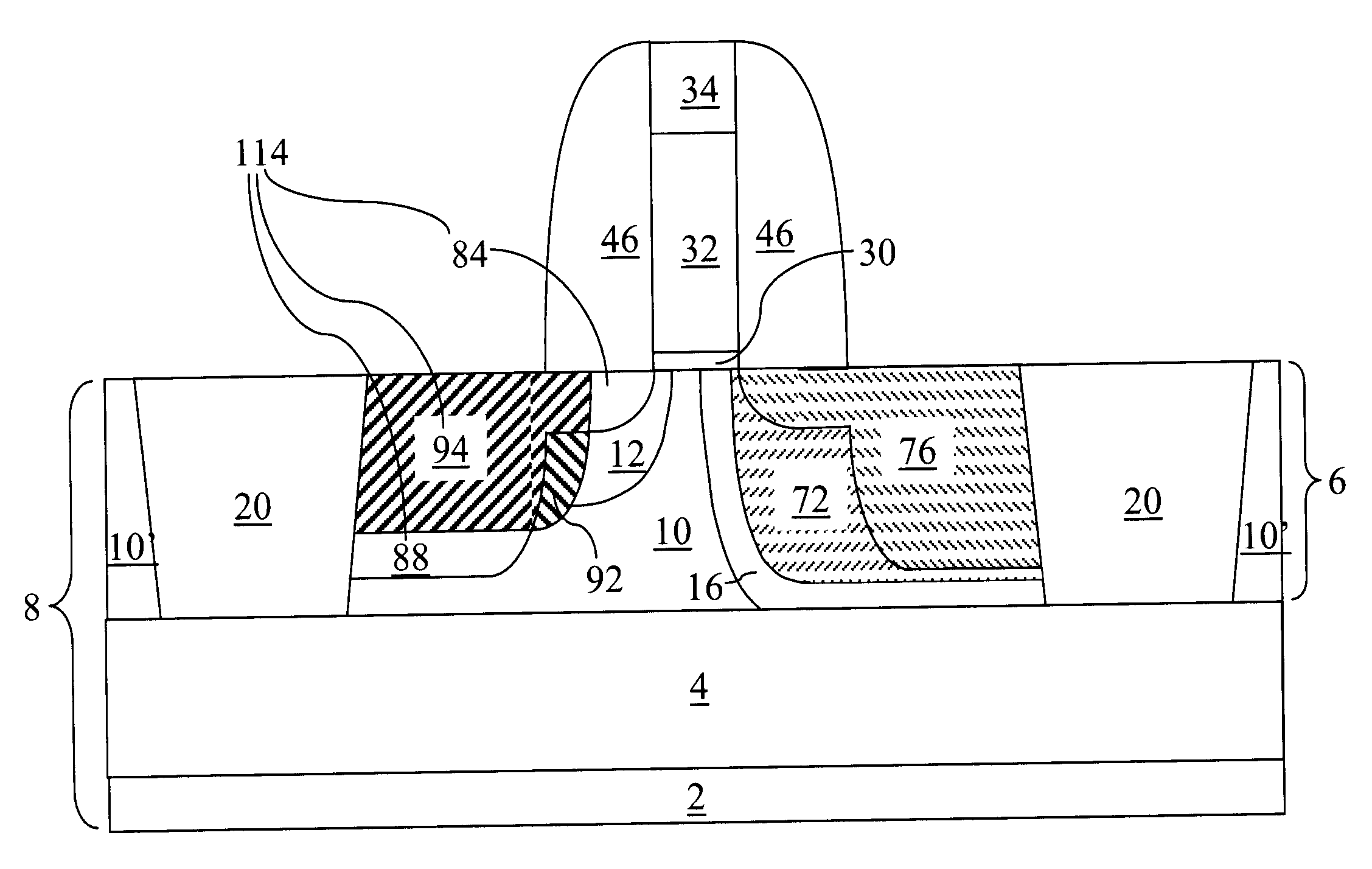
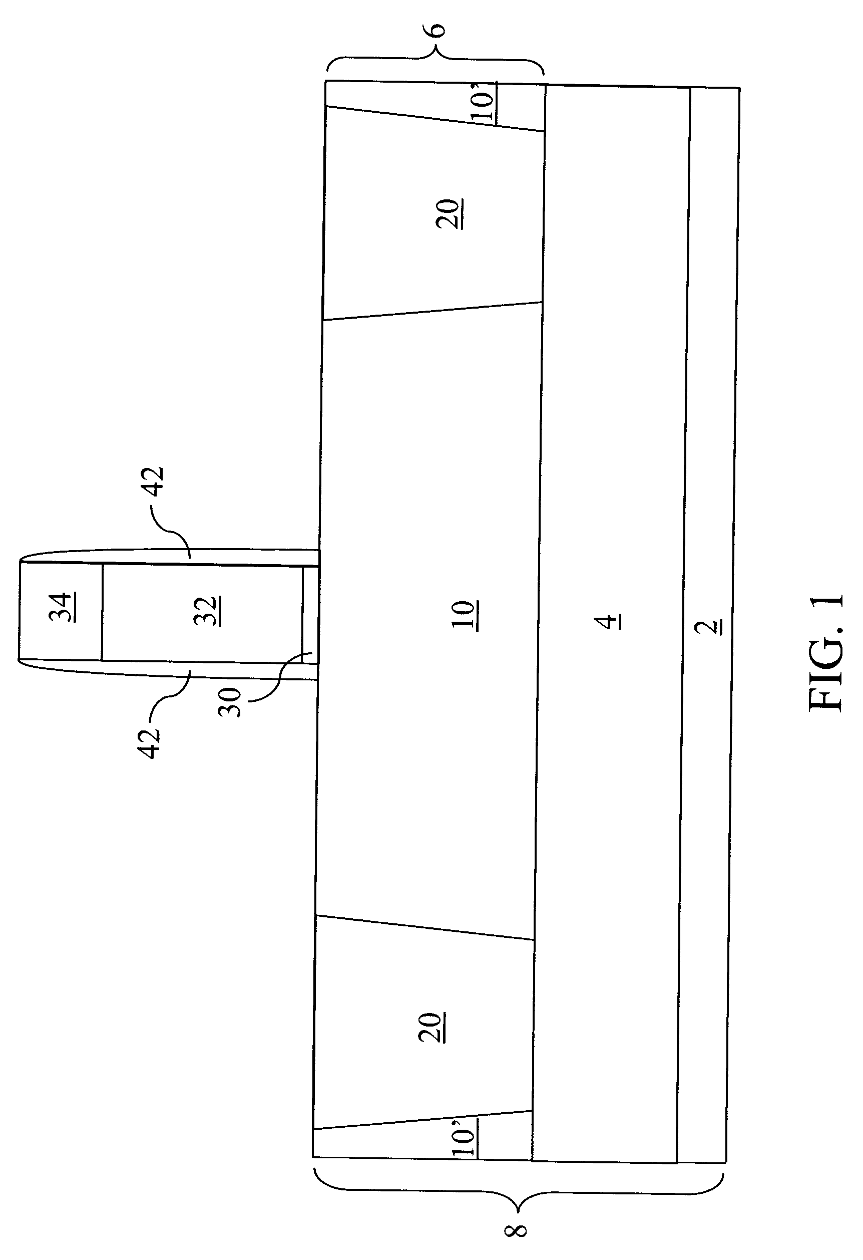
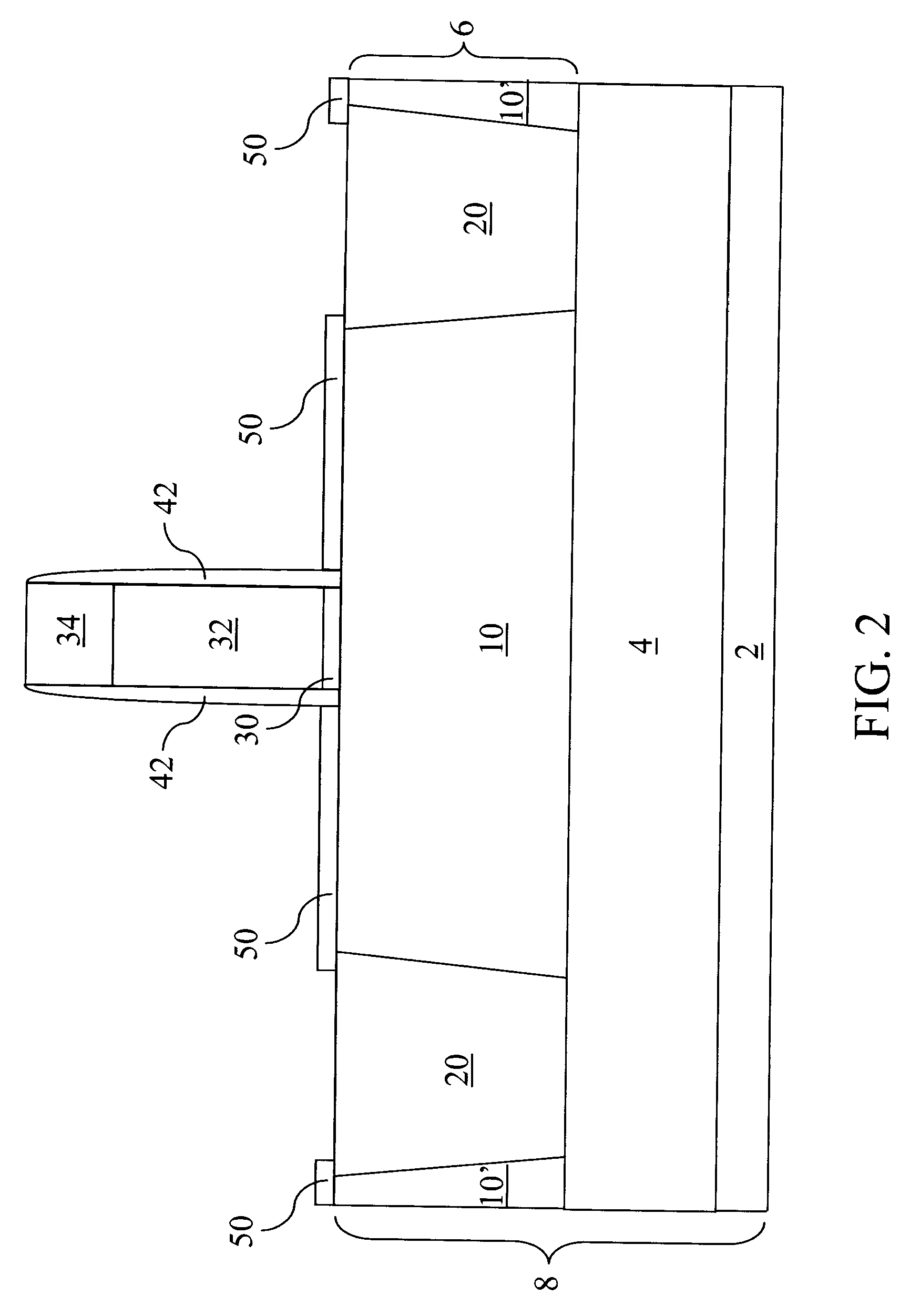
[0050]As stated above, the present invention relates to a metal oxide semiconductor field effect transistor (MOSFET) having a high breakdown voltage and methods of manufacturing the same, which are now described in detail with accompanying figures. It is noted that like and corresponding elements mentioned herein and illustrated in the drawings are referred to by like reference numerals.

[0051]Referring to FIG. 1, a first exemplary semiconductor structure according to the present invention comprises a substrate 8 and a gate structure formed thereupon. The substrate 8 includes a semiconductor region 10 that comprises silicon. The substrate 8 may be a semiconductor-on-insulator (SOI) substrate comprising a handle substrate 2, a buried insulator layer, and a top semiconductor layer 6. The top semiconductor structure contains the semiconductor region 10, a shallow trench isolation structure 20 laterally enclosing the semiconductor region 10, and at least another semiconductor region 10′....


PUM


Abstract

A field effect transistor comprising a silicon containing body is provided. After formation of a gate dielectric, gate electrode, and a first gate spacer, a drain side trench is formed and filled with a wide band gap semiconductor material. Optionally, a source side trench may be formed and filled with a silicon germanium alloy to enhance an on-current of the field effect transistor. Halo implantation and source and drain ion implantation are performed to form various doped regions. Since the wide band gap semiconductor material as a wider band gap than that of silicon, impact ionization is reduced due to the use of the wide band gap semiconductor material in the drain, and consequently, a breakdown voltage of the field effect transistor is increased compared to transistors employing silicon in the drain region.

Description

FIELD OF THE INVENTION[0001]The present invention relates to a semiconductor device, and particularly to a metal oxide semiconductor field effect transistor (MOSFET) having a high breakdown voltage and methods of manufacturing the same.BACKGROUND OF THE INVENTION[0002]On one hand, a metal oxide semiconductor field effect transistor (MOSFET) built on a silicon-on-insulator (SOI) substrate typically offers advantages over a MOSFET with comparable dimensions that is built on a bulk substrate by providing a higher on-current and lower parasitic capacitance between the body and other MOSFET components. On the other hand, a MOSFET built on an SOI substrate tends to have less consistency in the device operation due to “history effect,” or “floating body effect,” in which the potential of the body, and subsequently, the timing of the turn-on and the on-current of the SOI MOSFET are dependent on the past history of the SOI MOSFET. Furthermore, the level of leakage current also depends on the...

Claims


Application Information

Patent Timeline
IPC IPC(8): H01L29/786H01L21/336
CPCH01L21/26586H01L29/165H01L29/6653H01L29/7848H01L29/66659H01L29/7833H01L29/66636H01L29/7835H01L29/1045
Inventor KUMAR, ARVIND
Owner GLOBALFOUNDRIES INC
Why Eureka
Try Eureka