Semiconductor device and method for manufacturing semiconductor device

a semiconductor and semiconductor technology, applied in the field of semiconductor devices, can solve the problems of reducing yield, complicated steps of thin film transistors using polycrystalline semiconductor films, and limit the process temperature, and achieve the effects of reducing the fluctuation in the threshold of thin film transistors, excellent responsiveness as switching elements, and high speed operation

Inactive Publication Date: 2009-06-18
SEMICON ENERGY LAB CO LTD
View PDF38 Cites 29 Cited by
  • Summary
  • Abstract
  • Description
  • Claims
  • Application Information

AI Technical Summary

Benefits of technology

[0035]The thin film transistor using a YSZ film of the present invention has current-voltage characteristics represented by a curve with a steep slope in a rising portion, has excellent responsiveness as a switching element, and can be operated at high speed.
[0036]In the case of a light-emitting device using a thin film transistor using the YSZ film of the present invention, fluctuation in threshold of the thin film transistor can be reduced, which leads to improvement in reliability.
[0037]Further, in the case of a liquid crystal display device using the thin film transistor obtained by the manufacturing method of the present invention, field effect mobility can be increased and thus, the driving frequency of a driver circuit can be increased. Since the driver circuit can be operated at high speed, a frame frequency can be quadruplicated or black frames can be inserted.

Problems solved by technology

In the case of a thin film transistor using an amorphous semiconductor film, an amorphous semiconductor film such as a hydrogenated amorphous silicon film is used; therefore, there is limitation on the process temperature and heating at a temperature of 400° C. or higher at which hydrogen is desorbed from the film, intense laser light irradiation by which surface roughness is caused due to hydrogen in the film, and the like are not performed.
However, because of crystallization of a semiconductor film, steps of a thin film transistor using a polycrystalline semiconductor film are more complicated than steps of a thin film transistor using an amorphous semiconductor film.
Therefore, there occurs a problem in that yield is reduced and cost is increased.

Method used


Image

  • Semiconductor device and method for manufacturing semiconductor device
  • Semiconductor device and method for manufacturing semiconductor device
  • Semiconductor device and method for manufacturing semiconductor device

Examples


embodiment mode 1

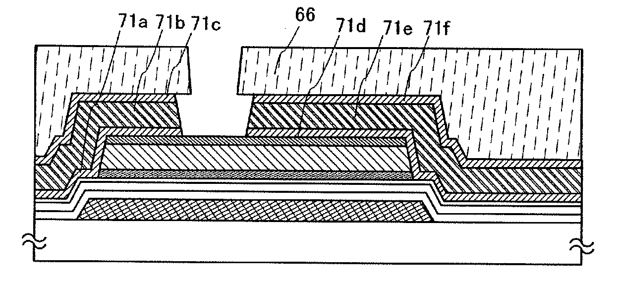
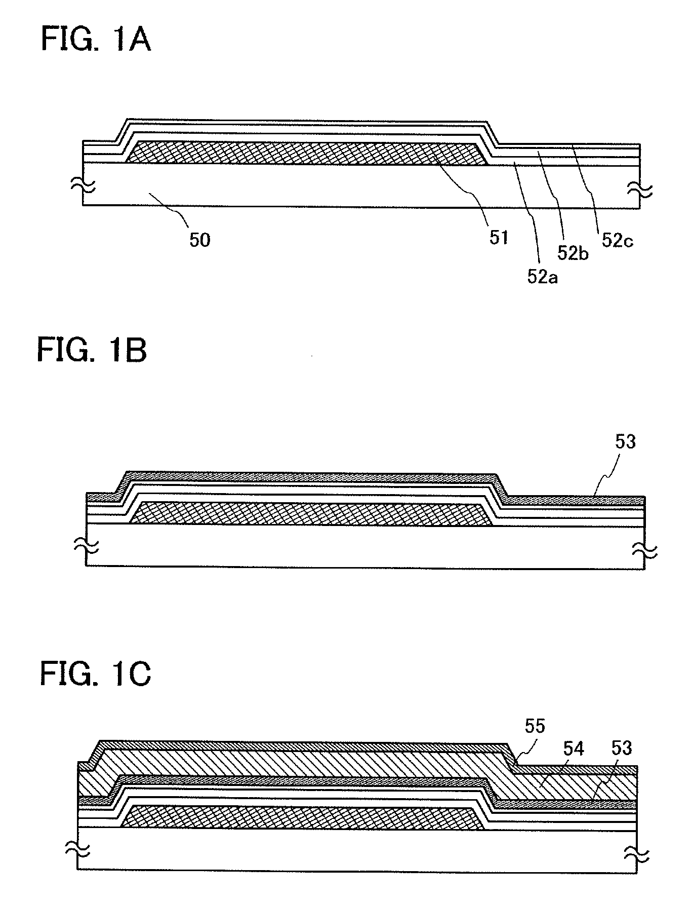
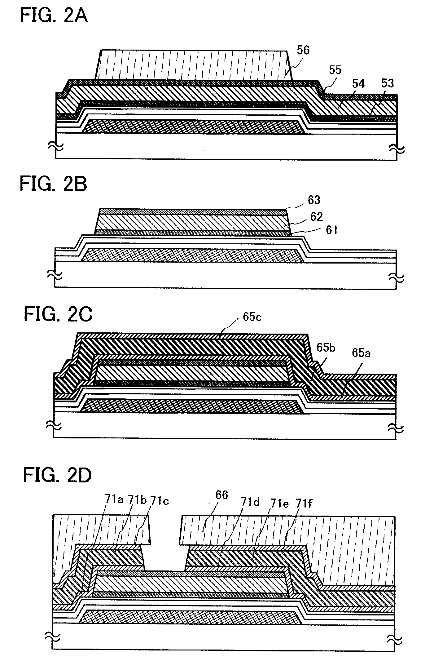
[0076]In this embodiment mode, an example in which the present invention is applied to a manufacturing process of a thin film transistor used for a liquid crystal display device is described with reference to FIGS. 1A to 1C, FIGS. 2A to 2D, FIGS. 3A to 3C, FIG. 4, FIGS. 5A and 5B, and FIGS. 6A and 6B. FIGS. 1A to 1C, FIGS. 2A to 2D, FIGS. 3A to 3C, FIGS. 5A and 5B, and FIGS. 6A and 6B are cross-sectional views illustrating manufacturing steps of a thin film transistor. FIG. 4 is a top view of a region where a thin film transistor and a pixel electrode are connected in one pixel.

[0077]As illustrated in FIG. 1A, a gate electrode 51 is formed over a substrate 50 having an insulating surface. As the substrate 50 having an insulating surface, a non-alkaline glass substrate manufactured by a fusion method or a float method, such as a barium borosilicate glass substrate, an aluminoborosilicate glass substrate, or an aluminosilicate glass substrate, or the like can be used. When the substra...

embodiment mode 2

[0128]Although a microcrystalline semiconductor film is formed to have a single-layer structure over a YSZ film formed as a gate insulating film in Embodiment Mode 1, any method for forming a microcrystalline semiconductor film can be used as long as a microcrystalline semiconductor film is formed using silicon having a lattice constant close to that of the YSZ. In Embodiment Mode 2, in order to improve the quality of a semiconductor region which is formed in the initial stage of deposition, a gate insulating film is formed over a gate electrode, a microcrystalline semiconductor film around an interface with the gate insulating film is formed under a first deposition condition in which a deposition rate is low but a high-quality film can be formed, and then, a microcrystalline semiconductor film is deposited under a second deposition condition in which a deposition rate is high. A deposition rate may be increased either stepwise or gradually. The manner in which the deposition rate ...

embodiment mode 3

[0145]In this embodiment mode, a method for forming a microcrystalline semiconductor film, which is different from that in Embodiment Mode 2, will be described. That is, a method for manufacturing a thin film transistor with excellent characteristics by a deposition method and a method for selecting a gas used for forming a microcrystalline semiconductor film by a plasma CVD method will be described.

[0146]In a method, the microcrystalline semiconductor film 23 obtained under the first deposition condition in Embodiment Mode 2 is made to have n-type conductivity, so that field effect mobility of the thin film transistor is improved. Specifically, an n-type impurity element is added in forming the microcrystalline semiconductor film under the first deposition condition. At that time, as the n-type impurity element, phosphorus, arsenic, or antimony can be used. In particular, phosphorus, which is available at low cost as a phosphine gas, is preferably used.

[0147]Further, by exposing a ...


PUM


Abstract

An object is to provide a semiconductor device including a microcrystalline semiconductor film with favorable quality and a method for manufacturing the semiconductor device. In a thin film transistor formed using a microcrystalline semiconductor film, yttria-stabilized zirconia having a fluorite structure is formed in the uppermost layer of a gate insulating film in order to improve quality of a microcrystalline semiconductor film to be formed in the initial stage of deposition. The microcrystalline semiconductor film is deposited on the yttria-stabilized zirconia, so that the microcrystalline semiconductor film around an interface with a base particularly has favorable crystallinity while by crystallinity of the base.

Description

BACKGROUND OF THE INVENTION[0001]1. Field of the Invention[0002]The present invention relates to a semiconductor device having a circuit which includes a thin film transistor, and a method for manufacturing the semiconductor device. For example, the present invention relates to an electronic appliance on which a light-emitting display device including an organic light-emitting element or an electro-optic device typified by a liquid crystal display panel is mounted as a component.[0003]Note that the term “semiconductor device” in this specification refers to a device in general that can operate by utilizing semiconductor characteristics, and an image display device, an electro-optic device, a semiconductor circuit, and an electronic appliance are all included in the semiconductor device.[0004]2. Description of the Related Art[0005]In recent years, a technique for forming thin film transistors (TFTs) each using a semiconductor thin film (a thickness of several nm to several hundred nm...

Claims


Application Information

Patent Timeline
Patent Type & Authority Applications(United States)
IPC IPC(8): H01L29/786H01L21/70H01L21/31
CPCH01L21/3105H01L21/31604H01L21/32055H01L29/78696H01L29/4908H01L29/66765H01L29/41733H01L21/02263
Inventor OHNUMA, HIDETOHIROSE, TAKASHI
Owner SEMICON ENERGY LAB CO LTD
Why Eureka
Try Eureka