Method and apparatus for dynamic characterization of reliability wearout mechanisms

a reliability wearout and dynamic characterization technology, applied in the direction of electrical testing, measurement devices, instruments, etc., can solve the problems of limiting the size reduction, the inability to arbitrarily reduce the size of individual circuit elements, and the current flow between the source and drain region blocked

Inactive Publication Date: 2009-07-02
GLOBALFOUNDRIES INC
View PDF3 Cites 26 Cited by
  • Summary
  • Abstract
  • Description
  • Claims
  • Application Information

AI Technical Summary

Benefits of technology

[0016]The present inventive technique specifically provides for a re-characterizing the DUT after a short, well-controlled time delay. This is to avoid the influence of “recovery effects” (self-“healing” behavior) in the characterization that would occur if a longer time period were allowed to pass before re-characterization.

Problems solved by technology

Conversely, when the applied gate voltage causes the conduction channel to disappear or “pinch off”, the FET device turns “off” and current flow between the source and drain regions is blocked.
The size of individual circuit elements cannot be reduced arbitrarily.
There are limitations to size reduction, including dimensional tolerance capabilities associated with manufacturing processes and various electrical phenomena that are associated with physical dimensions of circuit elements.
In addition, the essential requirement for high reliability of integrated circuits itself places limitations on shrinking the size of such elements.
The steps of identifying these and other limitations and discovering techniques for ameliorating these limitations have made possible the increasing complexity of integrated circuits.
As an example, the prior art in the field of manufacture, testing, and use of MOSFET devices has identified several problems that occur during long-term use of such devices.
NBTI in a MOSFET device is a serious detriment to the long-term stability of the MOSFET device.
The simultaneous demands for higher drive current at lower operating voltages has led to more serious concerns over negative bias temperature instability (NBTI), which significantly shifts threshold voltage and reduces drive current.
There are also indications that NBTI worsens exponentially with thinning gate oxide, and Vt (threshold voltage) shifts in the order of 50 mV are serious for devices operating at 1.2 V or below.
Recent experimental data suggest that the quasi static approximation may not be accurate in the case of NBTI due to recovery effects.
Using conventional prior-art stress / characterization techniques, considerable time can elapse between stress and measurement, resulting in mischaracterization of the rate of degradation and inaccurate device lifetime predictions.
Another problem with current accelerated aging techniques relates to the characterization of resistor / wire Electron Migration (EM) aging under AC condition.
This approach is severely limited by the bandwidth of the cabling used for wafer level testing permitting DC vs.
The current techniques used to characterize wearout have limitations that prevent a detailed characterization of both AC and DC wearout characteristics.

Method used


Image

  • Method and apparatus for dynamic characterization of reliability wearout mechanisms
  • Method and apparatus for dynamic characterization of reliability wearout mechanisms
  • Method and apparatus for dynamic characterization of reliability wearout mechanisms

Examples


Embodiment Construction

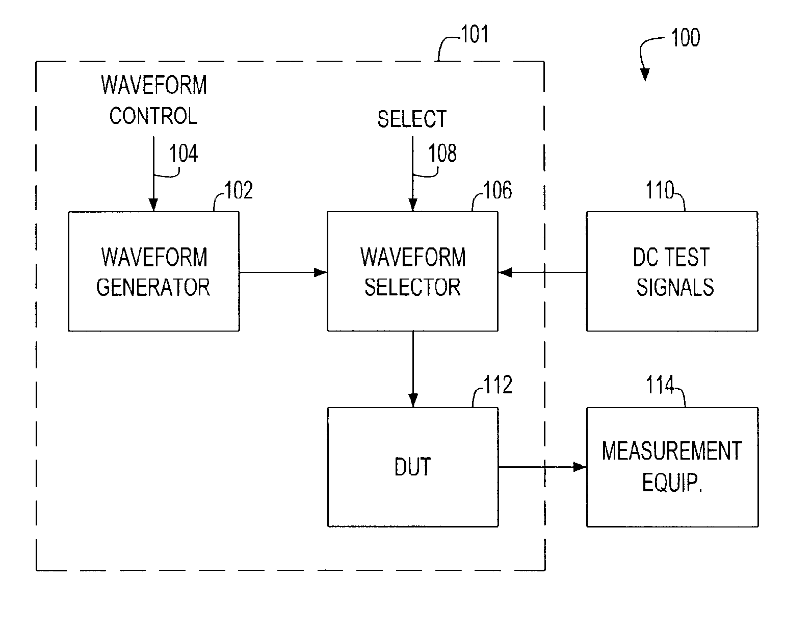
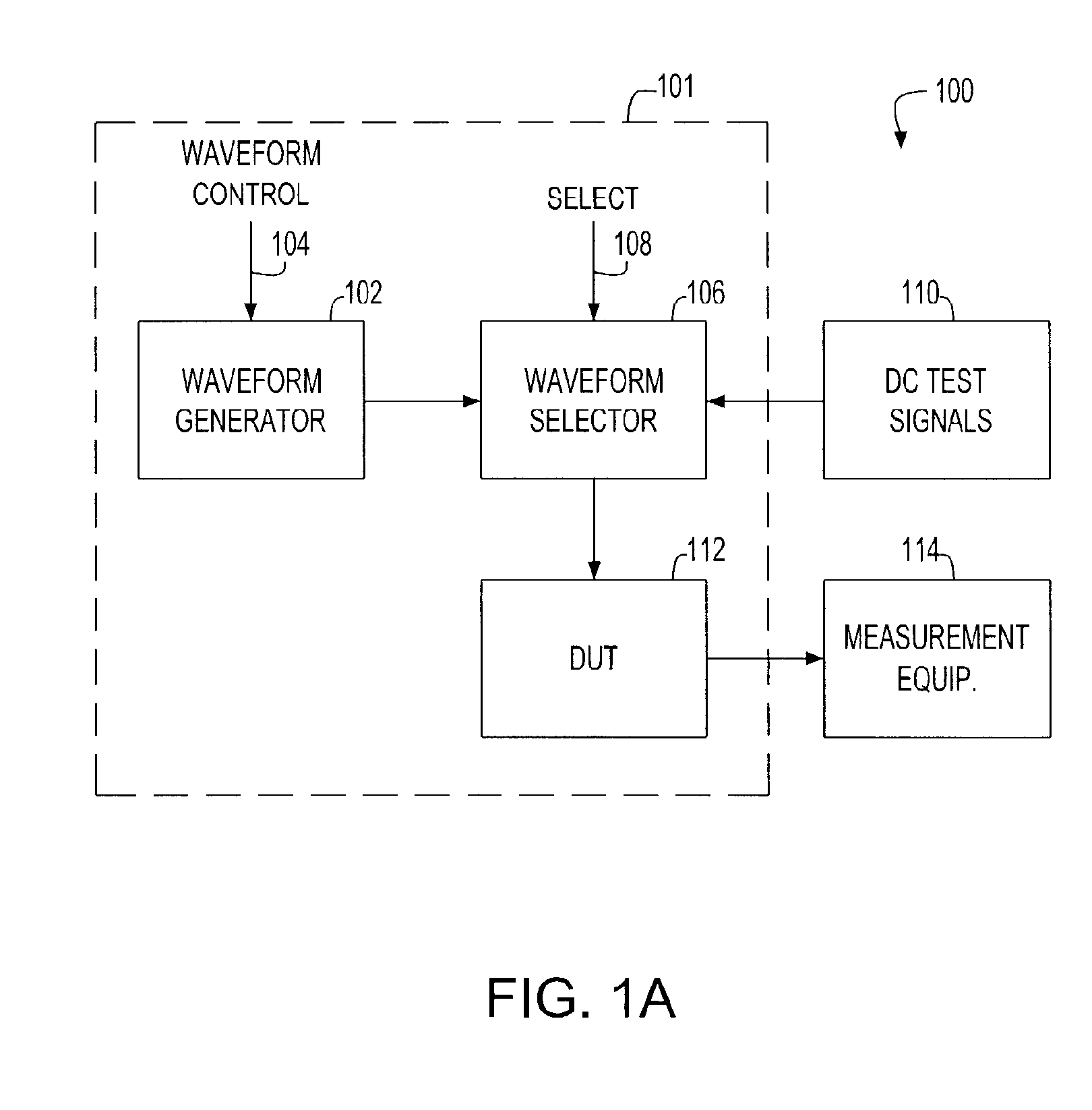
[0035]FIG. 1A is a block diagram of circuitry 100 for characterizing wearout mechanisms in integrated circuit devices, in accordance with the invention. On-chip elements of this circuitry 101 comprise a waveform generator 102, a waveform selector 106 and a device under test (DUT) 112. These on-chip elements 101 provide the ability to apply electrical stressing signals, particularly high-frequency AC stressing signals, to the device-under-test 112 (DUT) and to measure changes in the characteristics of the DUT in response to those stresses. The DUT 112 can be, e.g., a transistor, transmission gate, or resistive element. The waveform generator 102 produces a repeating AC waveform according to the states of a set of waveform control signals 104. The control signals 104 control the waveform generator 102 to produce specific desired signal characteristics (e.g., to produce a specific desired wave shape, amplitude, frequency and / or duty-cycle) for producing specific types of stresses relat...


PUM


Abstract

A method and apparatus for dynamic characterization of reliability wearout mechanisms is disclosed. The system comprises an integrated circuit incorporating a device under test to be measured, structure for inputting a waveform to the device under test for a first predetermined time interval, structure for disabling the inputting of the waveform to the device under test, structure for measuring one or more fundamental parameters of the device under test after a second predetermined time interval, and structure for calculating an aging estimate of the device under test without the influence of recovery effect based on the one or more measured fundamental parameters. The time between stressing and measurement is precisely controlled, providing for repeatable experiments, and serves to minimize measurement error caused by recovery effects.

Description

FIELD OF THE INVENTION[0001]The present invention relates generally to reliability testing of semiconductor devices and, more particularly, to an improved method and apparatus for dynamic characterization of reliability wearout mechanisms.BACKGROUND OF THE INVENTION[0002]There are two major types of FET (Field-Effect Transistor) devices, the metal-oxide-semiconductor field effect transistor or MOSFET (also called an insulated-gate FET, or IGFET), and the junction-gate FET, or JFET. An FET has a control gate and source and drain regions formed in a substrate. In MOSFETs, the control gate is formed above a thin dielectric insulator (gate dielectric) overlying a doped “channel” region between the source and drain regions. JFETs, like MOSFETs, have a doped channel region between their source and drain region but in JFETs, the control gate is formed by an oppositely doped gate region surrounding the channel region and forming a p-n junction therewith (hence the name “junction-gate” FET)....

Claims


Application Information

Patent Timeline
Patent Type & Authority Applications(United States)
IPC IPC(8): G01R31/02
CPCG01R31/2858G01R31/2856
Inventor LA ROSA, GIUSEPPEKOLVENBACH, KEVINWANG, PING-CHUANWYATT, STEPHEN D.
Owner GLOBALFOUNDRIES INC
Why Eureka
Try Eureka