
Eureka
For R&D, Eureka makes reading and utilizing patents & technical documents easy.
Eureka AIR
Designed for self-driven R&D workflows. Generate viable solutions, solve complex R&D challenges, empower your innovation with AI.

Eureka Materials
Designed for material experts only. Revolutionize your material R&D, from search, analyze, to developing new materials.

TechResearch
Generate reliable direction feasibility study reports for your R&D in just a few steps.

TechSeek
Discover and master advanced knowledge NOW. Basics, ideas, possibilities, all at once.

TechMind
As an expert in R&D Theories, TechMind can generates customized viable solutions instantly.

TechRisk
Analyze your overall solution with one click, know your potential R&D risks in advance.

TechMonitor
Get weekly tech updates, stay abreast of the latest tech innovations and key insights.
Metal chloride seeded growth of electronic and optical materials
- Summary
- Abstract
- Description
- Claims
- Application Information
AI Technical Summary
Problems solved by technology
Method used
Image

Examples
example 1
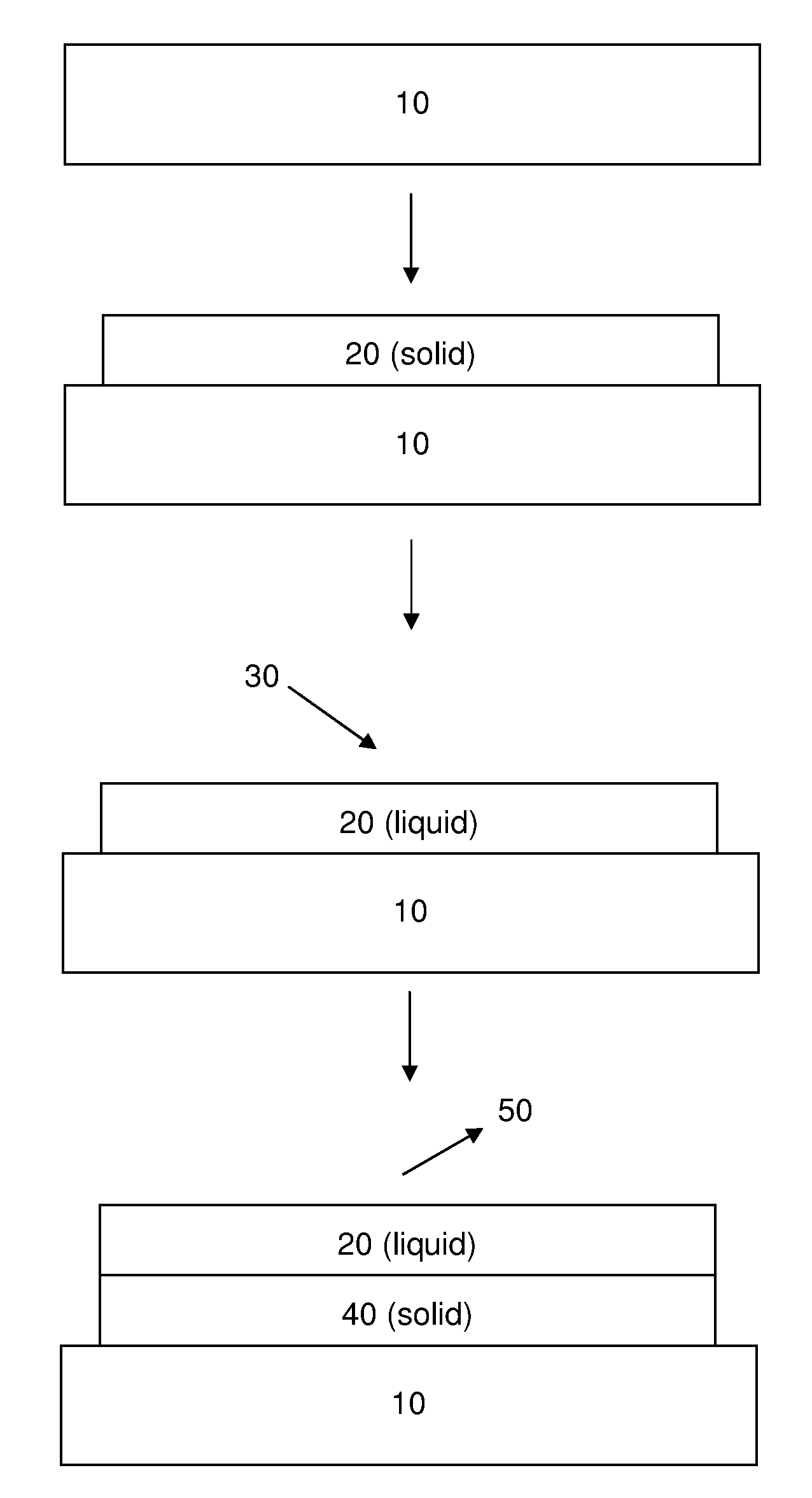
[0031]GaN with ErCl3 seeds on sapphire—GaN crystals were grown via an ErCl3 seed on c-, a- and r-plane sapphire substrates. The ErCl3 was dissolved into deionized water, then either dripped or spun onto the substrate. The substrate was heated to approximately 60° C. to drive off excess water, then loaded into a modified vertical impinging flow, metal organic chemical vapor deposition (MOCVD) reactor. A 50-Torr, H2 atmosphere was used during the ramp to growth temperature. Trimethylgallium was flowed for 2 s prior to the onset of NH3 flow to prevent nitridation of the Er seeds. A series of samples was produced for a growth duration of 1, 5, 10, 20, and 30 min. Results are presented for a growth temperature of 900° C. although this technique was demonstrated from 700 to 1050° C.
[0032]Structural characterization was performed with a Panalytical X'pert X-ray diffraction (XRD) system and a LEO FE Scanning Electron Microscope (SEM). The XRD characterization data can be considered as infor...
example 2
[0037]Additional characterization—GaN crystals were grown via an ErCl3 seed dispersed in a methanol solvent onto an a-plane sapphire substrates as described above. A LEO Field Emission Scanning Electron Microscope (SEM) and a FEI NOVA 200 SEM with energy dispersive x-ray (EDX) analysis was used to mill and analyze GaN micro-crystals. A Ga-ion beam was used to characterize the cross-section of GaN micro-crystal. A LabRam high resolution Jobin Yvon system fitted with a liquid nitrogen cooled CCD was employed for micro-Raman spectroscopy under backscattering geometry with a 632 nm He—Ne laser. The laser power was 0.6 mW at the sample surface after passing through the microscope internal optics. The sample was positioned by a motorized computer controlled stage.
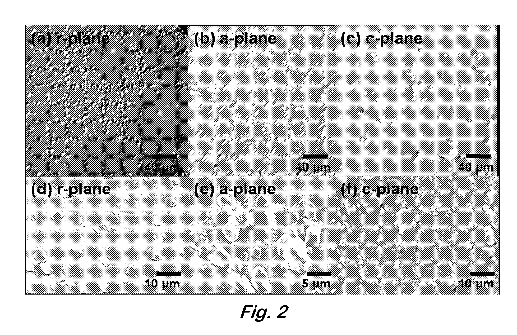
[0038]Bright field Normarski microscopy and electron micrographs in FIG. 8 reveal a high concentration of GaN crystals approximately 5-μm in length after 10 min of growth on a-plane sapphire. X-ray diffraction showed the growth d...
PUM
| Property | Measurement | Unit |
|---|---|---|
| Temperature | aaaaa | aaaaa |
| Temperature | aaaaa | aaaaa |
| Melting point | aaaaa | aaaaa |
Abstract
Description
Claims
Application Information
 - R&D Engineer
- R&D Manager
- IP Professional
- Industry Leading Data Capabilities
- Powerful AI technology
- Patent DNA Extraction
Browse by: Latest US Patents, China's latest patents, Technical Efficacy Thesaurus, Application Domain, Technology Topic, Popular Technical Reports.
© 2024 PatSnap. All rights reserved.Legal|Privacy policy|Modern Slavery Act Transparency Statement|Sitemap|About US| Contact US: help@patsnap.com