Method for bonding work pieces made of stainless steel, nickel or nickel alloys, using a bonding layer consisting of nickel-phosphorous, method for producing a micro-structured component using such method; micro-structured component obtained by such method

a technology of nickel-phosphorous and bonding layer, which is applied in the direction of microstructured components, non-electric welding apparatuses, microstructure devices, etc., can solve the problems of loss of dimensional accuracy of components, deformation or respectively distorted basic materials, and easy cracks in the structure of basic materials, so as to avoid local overheating and cracking, improve strength, and less suitable for dynamic loads

Inactive Publication Date: 2009-08-13
ATOTECH DEUT GMBH
View PDF9 Cites 19 Cited by
  • Summary
  • Abstract
  • Description
  • Claims
  • Application Information

AI Technical Summary

Benefits of technology

[0012]Consequently, modern process management attempts to avoid this “diffusion annealing” and to generate an extensively brittle-phase-free bonding zone through an optimised coordination between the solder / brazing-basic material combination and the process parameters. The aim is to make a soldering / brazing joint so narrow that the soldering / brazing joint clearance is below the critical soldering / brazing joint clearance (KLB) produced from the said coordination in the bonded component. The KLB indicates at which soldering / brazing joint clearance a largely brittle-phase-free soldering / brazing joint can be expected. Where nickel based solders are used the rule of thumb is KLB<50 μm and for nickel based solders containing phosphorous KLB<10 μm.
[0013]For example, W. Müller and J.-U. Müller, in Löttechnik—Leitfaden für die Praxis (Soldering / brazing—An Instruction Manual), Düsseldorf, 1995, Pages 167-170, state that it is not possible to obtain any notable improvement in strength through a post-tempering process or respectively a gap-minimising using nickel based solders containing phosphorous. The diffusion coefficients of the combination of phosphorous / basic material are considered be so small that the critical soldering / brazing joint clearances are far below 10 μm and could hardly be realised in practice. The components produced with nickel based solders containing phosphorous would consequently be less suitable for dynamic loads.
[0014]Soldering / brazing methods, however, from a production engineering and a cost point of view, provide some fundamental advantages, such as the possibility of using industrially produced presses, the possibility of being able to bond together even component layers with poor surface quality, to combine different materials together and to avoid local overheating and cracking in the basic material. In addition, numerous bonding regions on one component and consequently also components with large surface areas and comprising a plurality of individual functional layers can be bonded in one process step. Although soldering / brazing methods have been proposed many times already as a bonding method for micro-structured components, up to now there has been no success in using conventional soldering / brazing methods for the industrial production of such types of components, as additional requirements have to be met for their production compared to the diffusion welding method: On the one hand, no solder may pass into the micro-structured ducts in the component layers during the melting process and block the ducts. Contrary to many soldering / brazing methods, on the other hand, there must be no fluxing agent used as flux residue cannot be removed from the finished component or can only be removed at great expense. Flux residue not only presents unwanted contamination in the reactor, but is also the cause of corrosion. Particularly critical in this case are soldered / brazed joints on narrow webs in the component layers.
[0015]This is the reason why up to now components made from nickel, nickel alloys or stainless steel are preferably welded. The use of solder pastes, which are to be free of phosphorous in particular, is proposed as an alternative. Such solders comprise, for example, alloys that contain gold, cadmium, zinc and copper and are described in: Corrosion Resistant Alloys, Haynes International Inc. 2003, Page 16, in order to bond Hastelloy® alloys.
[0016]It is clear from the above embodiments that the expert would not use bonding layers made from nickel / phosphorous alloys to bond stainless steels, nickel or nickel alloys on account of the disadvantages described.
[0017]In the case of classic soldering / brazing, in dependence on the bonding temperature between soft-soldering (Tf<450° C., Tf: bonding temperature), brazing (450° C.<Tf<1100° C.) and high temperature brazing (Tf>950° C.), brazing is considered as a special case. Different solder materials are used, in this case, in the various temperature ranges. Their respective melting ranges are clearly more or less below that of the basic material to be bonded. When the soldering / brazing temperature has been obtained, the solder melts, wets the surfaces of the materials to be bonded and effects its adhesive connection once it has cooled. In classic soldering / brazing procedures, consequently, the solder layer formed in this manner always comprises a material that differs to that of the work pieces. The different physical characteristics resulting therefrom, of the solder on the one hand and of the basic material on the other, for instance different coefficients of thermal expansion, different electrochemical potentials and the different corrosion behaviour this leads to, different structures as well as the different hardness and ductility are fundamental disadvantages that are, however, more or less serious depending on the application and area of use of the component, that-is-to-say, they are acceptable disadvantages.

Problems solved by technology

To produce metal microstructured components, the thermal diffusion welding method is widely used as the bonding technology for the metal foils to be connected, as the welding methods referred to as alternatives do not provide any possibility of forming a complete bond on the faces of the foils that are usable for this purpose.
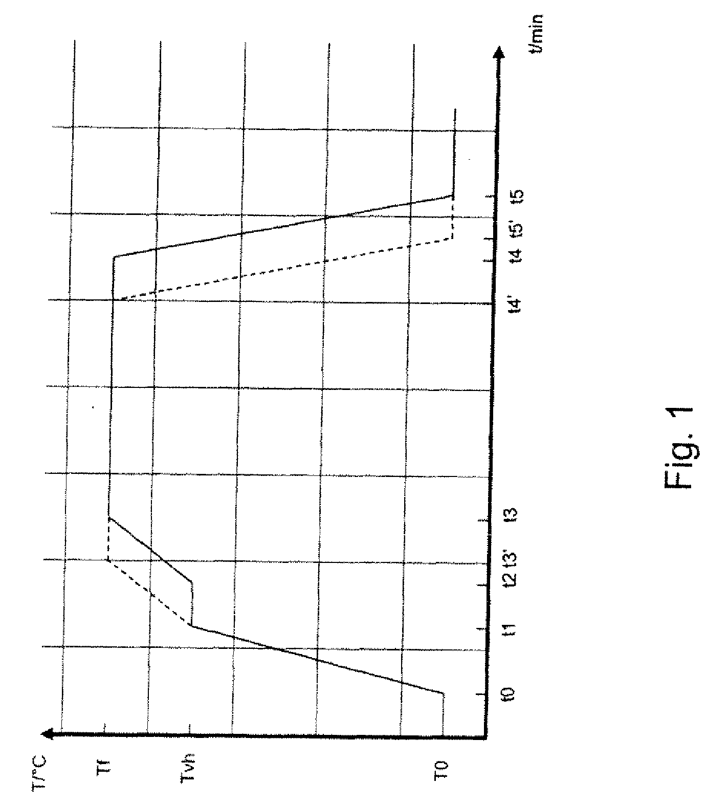
In the case of the said method, the addition of heat, and consequently the achievable bond of the foils together, are limited as regards location such that cracks can easily form in the structure of the basic material and the basic material can become deformed or respectively distorted through local overheating.
This leads to a loss in dimensional accuracy for the component.
However, this requirement is an important reason why micro-structured components are used in heat engineering, process engineering and chemical engineering, as conductive equilibrium in the component and the most precise temperature controls in chemical processes and reactions can only be guaranteed by means of a thermal coupling between the individual layers.
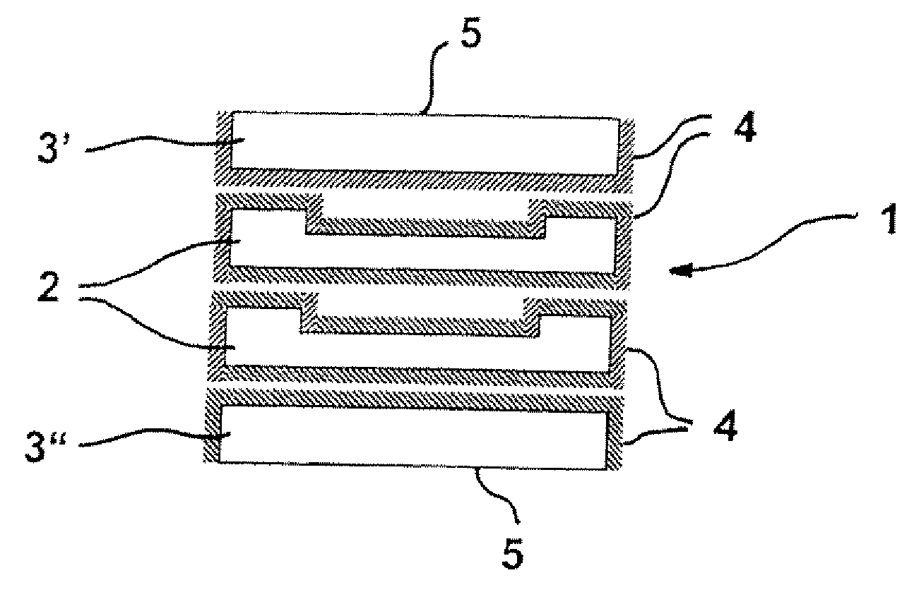
This means that a bonding layer is no longer recognisable in a cross section after the bonding method has been carried out, i.e., a bonding seam can no longer be visible.
In addition, there are restrictions on the selection of materials and on the combination of materials as, as a rule, where demands are made on the high temperature resistance of the basic material, the necessary minimum temperature during the diffusion welding process also rises.
More especially in the case of high temperature materials, the expenditure on hardware for diffusion welding rapidly becomes disproportionately high.
If, on account of the high temperature necessary, conventional press rams can no longer be used, fixing devices have to be employed.
Whereas the said method is still controllable in the case of small components with edge lengths of few centimetres, the difficulties with larger components very rapidly become insurmountable.
The reason for this is that it is no longer possible to obtain the absolutely necessary uniform distribution of contact pressure over the entire component.
Possible consequences are deformation of narrow webs between ducts in the component layers, distortion of the components and leakages.
The expenditure on hardware is high due to the combination of a very high temperature, pressure and high vacuum and is linked with a plurality of technical problems (no suitable commercial systems (high temperature pressing tools)).
Consequently, this method cannot be economically justified.
However, soldering methods always have the principle disadvantage that the solder, as the bonding layer between the component layers to be bonded, is produced from a material that is different to the material of the stacked layers.
The solder also introduces foreign materials which alter the characteristics of the basic material, such as strength and corrodibility or respectively corrosion resistance, and influence them in a negative manner.
A cause of this is, i.a. the formation of intermetallic phases during the soldering process, the number, size and distribution of which can negatively influence the characteristics of the basic material and consequently that of the bonded component in a lasting manner.
In the case of high temperature soldering, more especially with the use of nickel based solders, the formation of brittle hard phases presents a particular danger.
Thus additions of phosphorous, boron and carbon can result in the forming and stabilising of comparatively large amounts of brittle phases and consequently in the reducing of the ductility and strength as well as of the corrosion resistance of the basic materials.
This method of operation is in all cases connected to considerable extra costs, and disadvantageous effects, such as alloying the basic material or forming coarse grains, have definitely to be avoided.
To this may be added that it is not possible to check the completeness of the dissolution of the formed brittle phases in a non-destructive manner and that the basic materials have to be exposed to the high temperature after soldering has been performed.
The diffusion coefficients of the combination of phosphorous / basic material are considered be so small that the critical soldering / brazing joint clearances are far below 10 μm and could hardly be realised in practice.
The components produced with nickel based solders containing phosphorous would consequently be less suitable for dynamic loads.
Although soldering / brazing methods have been proposed many times already as a bonding method for micro-structured components, up to now there has been no success in using conventional soldering / brazing methods for the industrial production of such types of components, as additional requirements have to be met for their production compared to the diffusion welding method: On the one hand, no solder may pass into the micro-structured ducts in the component layers during the melting process and block the ducts.
Contrary to many soldering / brazing methods, on the other hand, there must be no fluxing agent used as flux residue cannot be removed from the finished component or can only be removed at great expense.
Flux residue not only presents unwanted contamination in the reactor, but is also the cause of corrosion.
The different physical characteristics resulting therefrom, of the solder on the one hand and of the basic material on the other, for instance different coefficients of thermal expansion, different electrochemical potentials and the different corrosion behaviour this leads to, different structures as well as the different hardness and ductility are fundamental disadvantages that are, however, more or less serious depending on the application and area of use of the component, that-is-to-say, they are acceptable disadvantages.
The fundamental problems that are produced when using a soldering / brazing method through the difference in the material between the bonding layer and the basic material cannot occur in the case of monolithically bonded components due to their nature.
Monolithic components, consequently, are generally only obtained by means of the afore-discussed difficult high temperature bonding method, such as the diffusion welding method, which is technically very time-consuming and expensive.
However, the bonded components are extraordinarily brittle as the structure formed in this case comprises an intermetallic phase.
Consequently, the formed bond has unsatisfactory material characteristics, more especially low mechanical strength under dynamic loads.

Method used


Image

  • Method for bonding work pieces made of stainless steel, nickel or nickel alloys, using a bonding layer consisting of nickel-phosphorous, method for producing a micro-structured component using such method; micro-structured component obtained by such method
  • Method for bonding work pieces made of stainless steel, nickel or nickel alloys, using a bonding layer consisting of nickel-phosphorous, method for producing a micro-structured component using such method; micro-structured component obtained by such method
  • Method for bonding work pieces made of stainless steel, nickel or nickel alloys, using a bonding layer consisting of nickel-phosphorous, method for producing a micro-structured component using such method; micro-structured component obtained by such method

Examples


example 1

[0093]Bonding sample cylinders made of Hastelloy® C-4:[0094]NiPx layer thickness: 3 μm[0095]Contact pressure: 1400 kPa[0096]Heat at 25 K / min to 1100° C.[0097]Hold at 1100° C. for 4 h[0098]Cool at 25 K / min

[0099]FIG. 2 shows a scanning electron microscopy image of the bonding zone obtained. There is no boundary face to be seen between the bonded cylinders. Consequently, this is a monolithic structure.

example 2

[0100]Bonding a Component Made from Hastelloy® C-4:[0101]NiPx layer thickness, 4.4 μm[0102]Contact pressure: 30 kPa[0103]Heat at 10 K / min to 800° C.[0104]Continue to heat at 5 K / min to 1100° C.[0105]Hold at 1100*C for 1 h[0106]Cool at 25 K / min

[0107]FIG. 3 shows a light-microscopy image of the bonding zone obtained. Apart from monolithic regions (right-hand side) small isolated deposits can also be seen (left-border). The said small island-like deposits do not compromise the material characteristics. The black dots on the image are artefacts caused by the preparation. Components bonded in this manner were air-tight and showed burst values in excess of 300 bar.

example 3

[0108]Bonding metal strips made from pure nickel:[0109]NiPx layer thickness: 4.8 μm[0110]Contact pressure: 30 kPa[0111]Heat at 10 K / min to 800° C.[0112]Heat further at 5 K / min to 1100° C.

[0113]Hold at 1100° C. for 1 h[0114]Cool at 25 K / min

[0115]FIG. 4 shows a light microscopy image of the bonding zone. The boundary face is no longer visible. Consequently, this is a monolithic bonding seam.


PUM

PropertyMeasurementUnit
thicknessaaaaaaaaaa
contact pressureaaaaaaaaaa
thicknessaaaaaaaaaa

Abstract

To form high performance bonding connections suitable for producing micro-structured components made of a plurality of individual layers, bonding by the steps; providing at least two work pieces; forming a metal bonding layer on at least one side of at least one of said at least two work pieces by chemical or electrolytic metal plating method; the metal bonding layer being a nickel/phosphorous alloy having a prescribed phosphorous content and prescribed thickness; forming a bonding arrangement comprising said work pieces so that there is at least one metal bonding layer between said at least two respective work pieces; heating at a prescribed heating rate to a temperature above the melting temperature of the bonding layer; bonding the two work pieces by applying contact pressure within a prescribed range; and cooling at a prescribed rate.

Description

FIELD OF THE INVENTION[0001]The present invention relates to a method for bonding at least two work pieces made of stainless steel, nickel or nickel alloys and to a method for producing a micro structured component, selected from the group including micro-reactors, micro-heat exchangers, micro-coolers and micro-mixers. In addition, the invention relates to a microstructured component, i.e., a component with fluid structures, comprising a stack of microstructured component layers made of stainless steel, nickel or nickel alloys, which are interconnected.STATE OF THE ART[0002]Nickel alloys include, i.a., nickel / chromium alloys, which contain less than 50% by weight iron. The said alloys are no longer considered as steels but as so-called super alloys. They are characterised by a particular corrosion resistance and high temperature stability (so-called high temperature alloys) and are based on the alloy type NiCr8020 first described in 1906 (composition: 80% by weight nickel, 20% by we...

Claims


Application Information

Patent Timeline
Patent Type & Authority Applications(United States)
IPC IPC(8): B32B15/18B23K31/02
CPCB23K20/023B23K20/227B23K20/233B23K2201/045B23K2201/14B23K2201/185Y10T428/12646B23K2203/08B81C3/001B81C2203/035F28D9/00F28F2260/02B23K2203/02B23K2101/045B23K2101/14B23K2101/185B23K2103/05B23K2103/26
Inventor HERBER, RALPHKURTZ, OLAFETZKORN, JOHANNESMADRY, CHRISTIANSCHWIEKENDICK, CARSTENSCHAFER, GERD
Owner ATOTECH DEUT GMBH
Why Eureka
Try Eureka