

Formation of clean interfacial thin film solar cells
a technology of interfacial thin film and solar cells, which is applied in the direction of coating, chemical vapor deposition coating, plasma technique, etc., can solve the problems of increasing weight, complex structure design of solar cells, and inability to meet the needs of solar cells, so as to reduce the cost of chamber cleaning gas, reduce the production time required, and reduce the risk
- Summary
- Abstract
- Description
- Claims
- Application Information
AI Technical Summary
Benefits of technology
Problems solved by technology
Method used
Image

Examples
example one
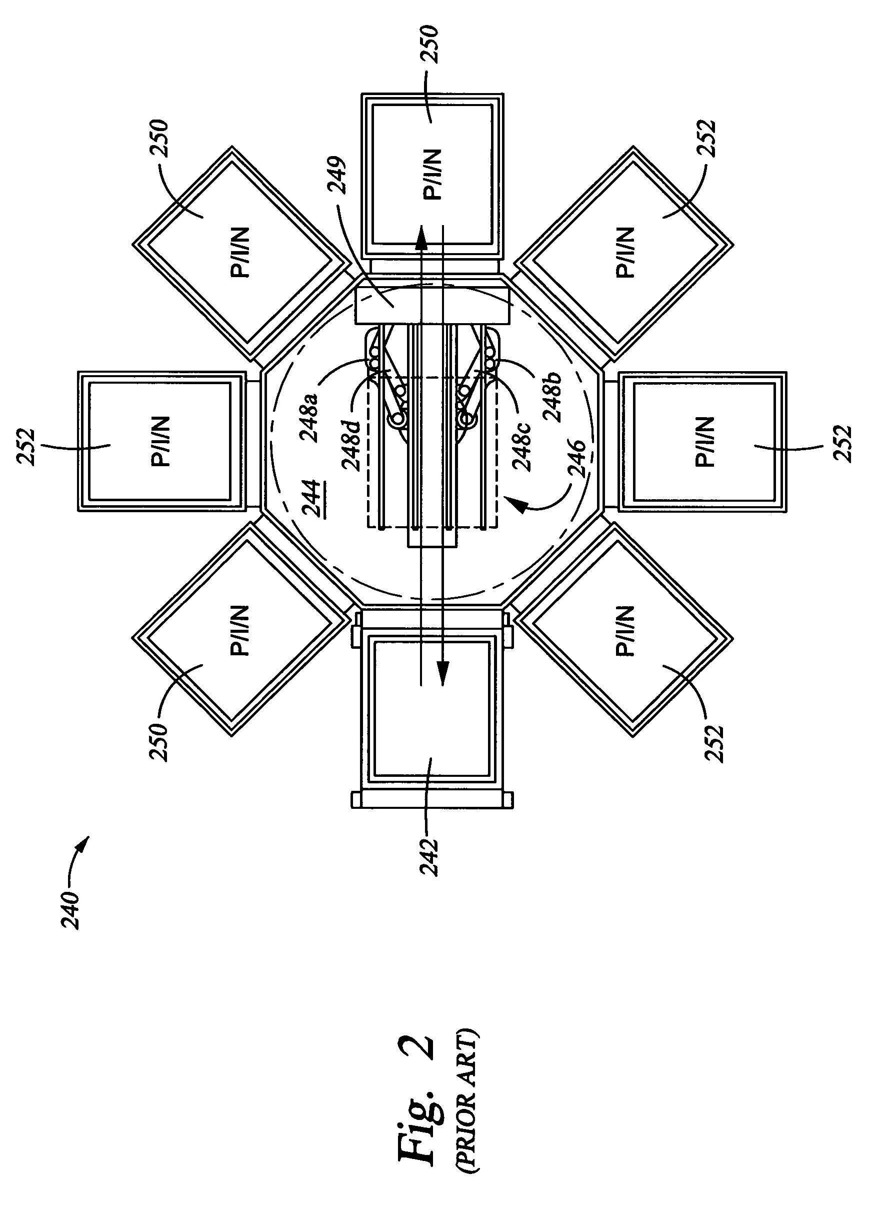
[0043]FIG. 2 shows an comparative exemplary “single” chamber process system 240. While a similar processing system could be used to produce a solar cell configuration other than a PIN configuration, for purposes of discussion in general, this layer configuration is described. One of skill in the art can extend the concepts described herein to structures other than those having a PIN configuration.
[0044]In a “single” chamber PIN configuration processing method, all of the p, i, and n layers of a PIN solar cell are deposited in a single process chamber. The method includes the following steps: a) providing a single PECVD processing chamber configured to deposit a p-doped layer, an intrinsic layer, and an n-doped layer; b) placing a substrate having a surface area of 1,000,000 mm2 or larger within the PECVD processing chamber; c) forming at least one p-doped layer upon the substrate; d) forming at least one intrinsic layer overlying the p-doped layer; and e) forming at least one n-dope...
example two
[0048]FIG. 3A shows a comparative “two” chamber design PECVD cluster processing system 300. This embodiment includes five processing chambers. The p-doped layer is deposited in one chamber, while the i-layer and n-doped layer are deposited in a single additional chamber. In particular, the processing chamber 304 is capable of depositing the p-doped layer which typically contains amorphous silicon, but which may also contain microcrystalline silicon or polycrystalline silicon. The i-layer and the n-doped layer may be deposited in process chambers 306a) through 306d). The length of the distances 332 and 334 illustrated on FIG. 3A are such that the central substrate transfer robot 308 can work more efficiently. The central substrate transfer robot 308 may be a dual armed robot of the kind described with reference to the central substrate transfer robot 246 shown in FIG. 2. An example of a commercially available “two” chamber design, multi-chambered processing system, for processing of ...
example three
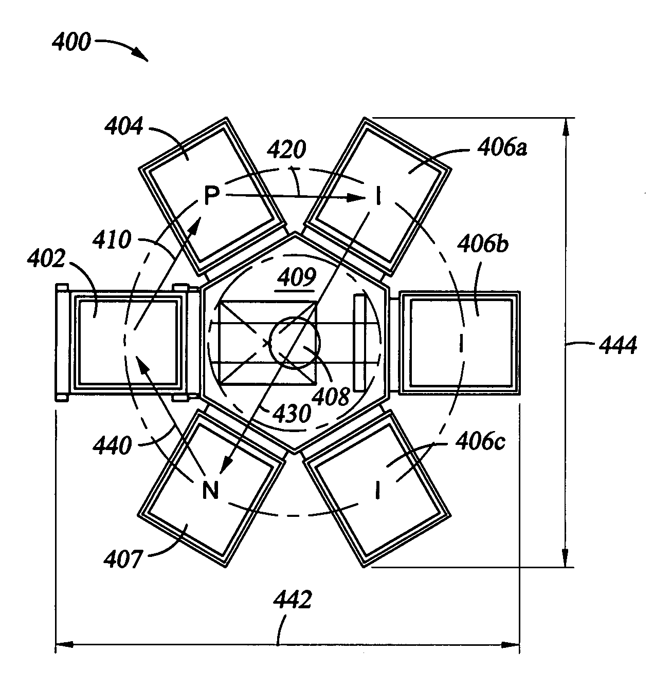
[0054]FIG. 4A shows a “three” chamber design of a multi-chamber PECVD cluster processing system 400 of the kind which may be used to practice embodiments of the present invention. This cluster processing system is referred to as a “three” chamber process apparatus because each different kind of layer is deposited in a separate chamber. The three chamber processing system includes a load lock docking chamber 402 and five film / layer-depositing chambers. One film-forming chamber 404 is capable of depositing a p-doped layer; three film-forming chambers 406a-406c, are capable of depositing an i-layer; and one film-forming chamber 407 is capable of depositing an n-doped layer. The cluster processing system includes a load lock docking chamber 402, and five film deposition chambers of the kind shown in FIG. 1, arranged around a transfer chamber 409 which contains a central substrate transfer robot 408. The central substrate transfer robot 408 is advantageously a dual arm transfer robot of ...
PUM
| Property | Measurement | Unit |
|---|---|---|
| Time | aaaaa | aaaaa |
| Area | aaaaa | aaaaa |
| Thickness | aaaaa | aaaaa |
Abstract
Description
Claims
Application Information