Probe of cantilever probe card

a cantilever probe and probe technology, applied in the field of probes of cantilever probe cards, can solve the problems of affecting the manufacture cost, unable to achieve cost reduction, and enormous manpower and working hours in assembly and fabrication of the present cantilever probe cards, so as to achieve stable electro-conductivity, reduce contact force, and prolong the life of the cantilever probe cards

Inactive Publication Date: 2009-08-27
IPWORKS TECH CORP
View PDF2 Cites 26 Cited by
  • Summary
  • Abstract
  • Description
  • Claims
  • Application Information

AI Technical Summary

Benefits of technology

[0009]An object of the present invention is to provide a probe of a cantilever probe card, which is used to maintain the test quality of the wafer probing test, and to prevent the probe from being wetted with a to-be-tested die, so as to decrease the cleaning frequency of the probe, moreover, to enhance the uptime of test machines, and to increase the test yield of the dies for ultimately reducing the entire test cost.
[0013]Comparing with prior arts, the present invention can efficiently provide an excellent advantages of no-clean, consisting and stable electro-conductivity, lower contact force and longer lifetime cantilever probe card because there is a nano-film of high electro-conductive nanomaterial coated on the probe tip. Moreover, the probe of the present invention maintains the test quality of the wafer probing test by preventing from generating excessive attraction force between each probe and each pad of the aforesaid to-be-tested die. Accordingly, the cleaning frequency of the probe can be decreased, moreover, the uptime of test machines can be increased and consequently, the test yield of the dies is increased for ultimately reducing the entire test cost.

Problems solved by technology

Thus, a wafer probing test is one of important processes in the integrated circuit fabrication, which affects the manufacture cost thereof.
The assembly and fabrication of the present cantilever probe card takes tremendous manpower and working hours.
So, cost down cannot be achieved because mass production is not possible, either.
Accordingly, maintaining good test yield and great test stability becomes quite difficult when tests for several to-be-tested dies are executed simultaneously.
After the tip numerously scratch the surface of the to-be-tested die, the tip of the probe may be wetted with foreign matter (such as solder from the pad), the test quality may be lowered or the mis-test probability may be increased, to result in low test yield unexpectedly.
Nevertheless, the minimum overdrive contact force may damage other lower structure under the surface of the pad of the to-be-tested die.
However, with the gradually increasing number of the probes or the gradually decreasing pitch between the adjacent probes, the cleaning frequency of the probes may be considerably increased, disadvantages of consequentially lowering the uptime of test machines and shortening the lifetime of the probes appear to under the aforesaid gradual changes.
The foregoing solder-wetted problem is generally occurred on the probes of the cantilever probe card.
Recently, although related manufacturers develop a kind of probe coated with a metal film capable of extending the lifetime thereof but the wetted problem still cannot be solved.
As a result, the metal film still cannot enhance the test yield and the test stability.

Method used


Image

  • Probe of cantilever probe card
  • Probe of cantilever probe card
  • Probe of cantilever probe card

Examples


Embodiment Construction

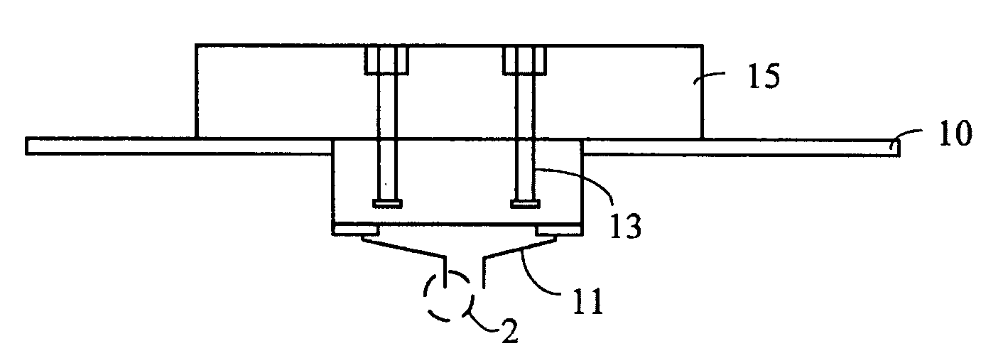
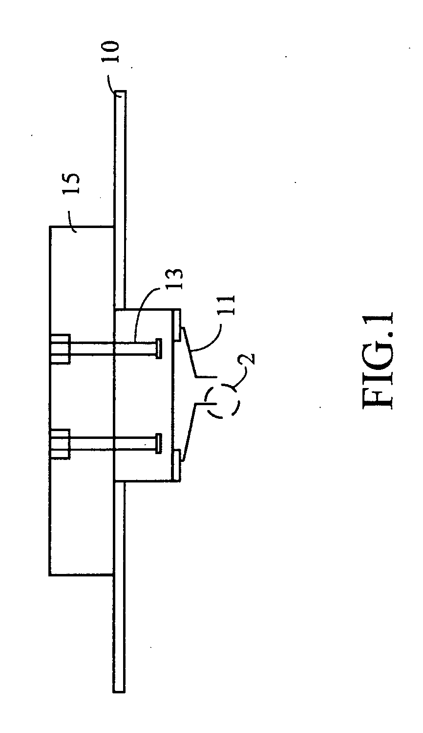
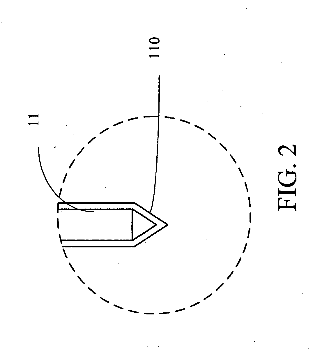
[0016]The present invention discloses a probe of a cantilever probe card, which having a plurality of probes mounted thereon. The probe is made of a metal material and a nano-film of electro-conductive nanomaterial is coated on the probe.

[0017]The aforesaid nano-film of electro-conductive nanomaterial can be polypyrrole, polyparaphenylene, polythiophene, polyaniline, combination thereof, or derivative thereof. The thickness of the nano-film of electro-conductive nanomaterial can be such as 1-20 nm. Further, the thickness of the nano-film of electro-conductive nanomaterial can be such as 1-5 nm.

[0018]The metal material can be nickel, gold, copper, tungsten, rhenium, titanium, beryllium, palladium, platinum, silver, zinc, electro-conductive metal, or alloy thereof. The rhenium-tungsten alloy or the beryllium-copper alloy can be illustrated. Furthermore, the probe can be a metal micro-spring or a metal pin.

[0019]Moreover, the nano-film of electro-conductive nanomaterial can be coated o...


PUM


Abstract

A probe of a cantilever probe card (Epoxy probe card) is disclosed. The probe has a tip and a surface region extended from the tip of the probe about 5-10 mil is coated with a nano-film of high electro-conductive nanomaterial. The thickness of the nano-film is about 1-20 nm. Through the coating process, the nano-film coated on the probe of the cantilever probe card can efficiently provide the excellent advantages of no-clean, stable electro-conductivity, minimum overdrive force and longer usage lifetime for the probe of cantilever probe card. Accordingly, the yield of wafer testing can be improved and the frequency of cleaning the probe can be decreased. Furthermore, the total testing cost can be reduced.

Description

BACKGROUND OF THE INVENTION[0001]1. Field of the Invention[0002]The present invention relates to a probe of a probe card for a wafer probing test, and more particularly to a probe of a cantilever probe card having a nano-film of electro-conductive nanomaterial on the probe.[0003]2. Description of Prior Art[0004]A probe card is constructed by a multi-layer printed circuit board (PCB) which may include more than 30 layers. The probe card has complicated structure and provides a plurality of probes for being in contact with a plurality of electrical contacts (i.e. pads) on a wafer, respectively. Generally, a contact area between each of the probes and each of the electrical contacts of the wafer is smaller than a cross-sectional area of one hair. Before an integrated circuit (IC) die is packaged by encapsulant, the probe card can be used to test electrical functions of the IC die cut from a wafer, in order to remove defective dies and keep known good dies for the following packaging pr...

Claims


Application Information

Patent Timeline
Patent Type & Authority Applications(United States)
IPC IPC(8): G01R1/067
CPCG01R1/06727G01R3/00G01R1/06755
Inventor CHEN, BEEN-LONGCHEN, HUANG-CHIH
Owner IPWORKS TECH CORP
Why Eureka
Try Eureka