Silicon substrate for magnetic recording and method for manufacturing the same

a technology of silicon substrate and magnetic recording, which is applied in the direction of manufacturing tools, lapping machines, instruments, etc., can solve the problems of high cost of single crystalline si wafers of 48 mm diameter or larger, and achieve the effects of improving the strength of thin plates, high cost performance, and surface flatness and smoothness

Inactive Publication Date: 2009-09-03
SHIN ETSU CHEM IND CO LTD
View PDF8 Cites 4 Cited by
  • Summary
  • Abstract
  • Description
  • Claims
  • Application Information

AI Technical Summary

Benefits of technology

[0036]By forming and polishing the silicon film thereon, the silicon substrate for magnetic recording or a magnetic recording medium may achieve surface flatness and smoothness, the improved strength of the thin plat

Problems solved by technology

However, the only weak point is the high costs of the

Method used


Image

  • Silicon substrate for magnetic recording and method for manufacturing the same
  • Silicon substrate for magnetic recording and method for manufacturing the same
  • Silicon substrate for magnetic recording and method for manufacturing the same

Examples


examples 1 to 7

[0065]Wafer of polycrystalline Si each having a “five-nines” purity (156 mm square, 0.6 mm thickness) was prepared (S1). From the polycrystalline Si wafers, Si substrates each having an outside diameter of 65 mm and an inside diameter of 20 mm were core-cutted using a laser processing machine (YAG laser, 1064 nm wavelength) to obtain four substrates per wafer (S2). These substrates were subjected to inside / outside coring (S3), thickness adjustment (S4), and end surface polishing (S5).

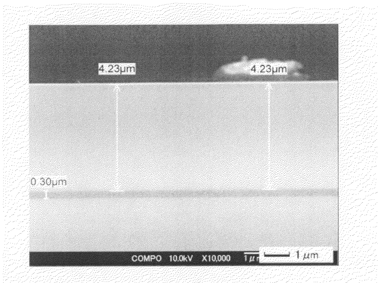
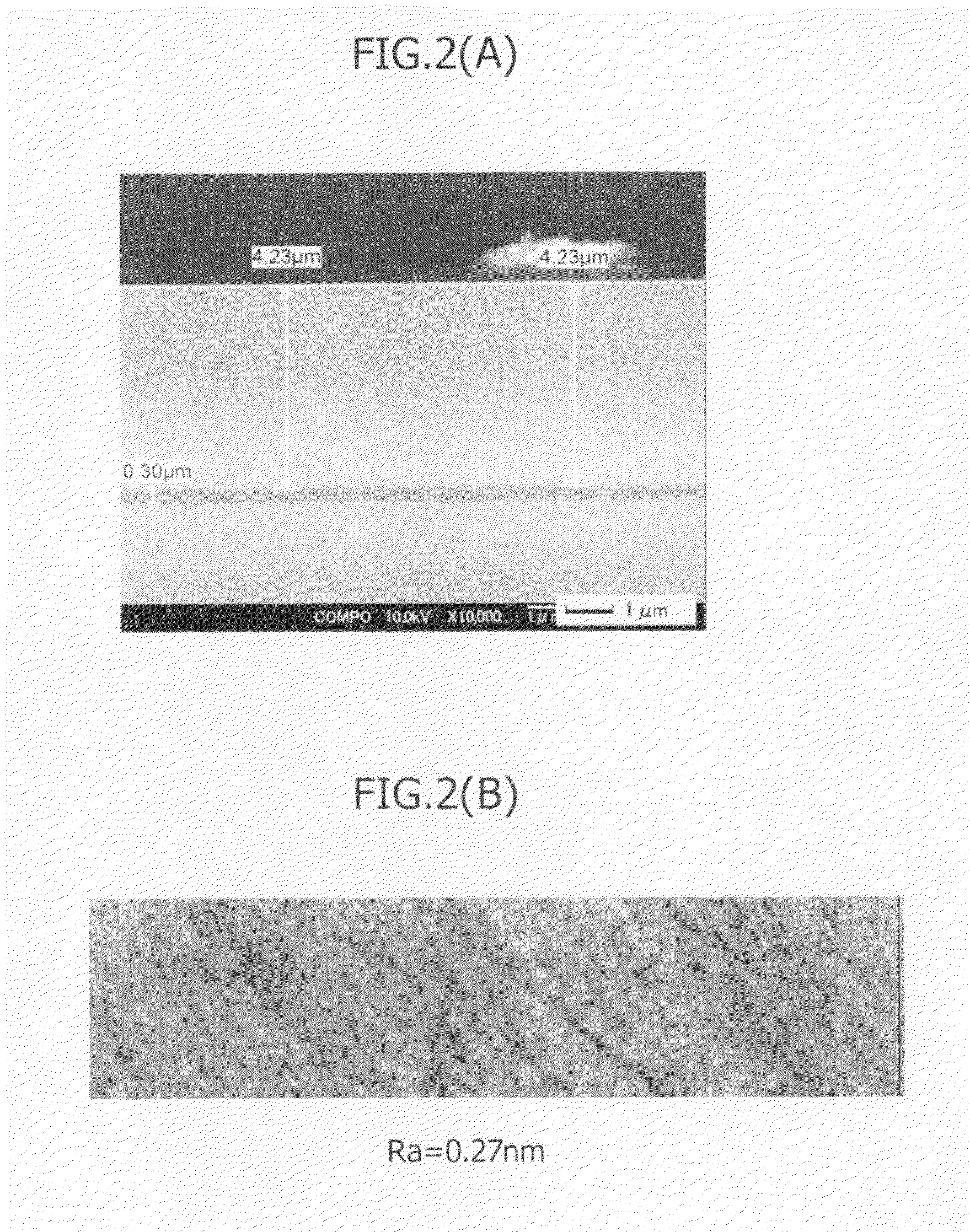
[0066]Next, rough polishing was performed on the major surfaces of the polycrystalline silicon substrate (S6). The rough polishing was performed by a double-sided polisher using a slurry of colloidal silica having a pH of 8.5 (an average particle diameter of 40 nm) under a polishing pressure of 10 kg / cm2 for 10 to 30 minutes by a maximum of 1500 nm. The inter-grain step in the major surface of the Si substrate after rough polishing, measured by an optical tester (Zygo) was about 5 nm.

[0067]An amorphous ...


PUM

PropertyMeasurementUnit
Thicknessaaaaaaaaaa
Thicknessaaaaaaaaaa
Surface roughnessaaaaaaaaaa

Abstract

There is provided a silicon substrate for magnetic recording that does not make the process for forming a magnetic recording layer complicated, excels in surface flatness, and has a thermal conductivity equivalent to the thermal conductivity of a single crystalline or polycrystalline bulk substrate. After forming a thin Silicon film on the surface of a polycrystalline silicon substrate subjected to rough polishing (S6), the silicon film is subjected to precision polishing (S8) such as CMP polishing to raise the flatness of the substrate. Thereby, a flat and smooth surface can be obtained without being affected by difference in the crystal orientation of polycrystalline grains and the presence of crystalline grain boundary, and a thermal conductivity equivalent to the thermal conductivity of a bulk Si substrate can be achieved.

Description

CROSS-RELATED APPLICATIONS[0001]This application claims priority from Japanese Patent Application No. 2008-037166; filed Feb. 19, 2008, the disclosure of which is incorporated herein by reference in its entirety.BACKGROUND OF THE INVENTION[0002]1. Field of the Invention[0003]The present invention relates to a polycrystalline silicon substrate used for magnetic recording, and a method for manufacturing the same.[0004]2. Description of the Related Art[0005]In the technical field of magnetic recording, a hard disk device has been essential as a primary external recording device suitable for electronic devices such as personal computers. A hard disk is incorporated into the hard disk device as a magnetic recording medium, and conventional hard disks have adopted a system known as the “in-plane magnetic recording system (horizontal magnetic recording system)” in which magnetic information is written horizontally on the disk surface.[0006]FIG. 3(A) is a schematic sectional view for illust...

Claims


Application Information

Patent Timeline
IPC IPC(8): G11B5/00B24B1/00B24B7/24
CPCB24B37/04G11B5/7315G11B2005/0021G11B5/8404G11B5/82G11B5/73915
Inventor OHASHI, KEN
Owner SHIN ETSU CHEM IND CO LTD
Why Eureka
Try Eureka