CMOS image sensor with reduced dark current

a technology of image sensor and dark current, applied in the field of semiconductor image sensor structure, can solve the problems of reducing the dynamic range, reducing the charge capacity, and reducing the image quality of the cmos image sensor, and achieve the effect of enhancing the performance of the photodiode and reducing the dark curren

Active Publication Date: 2009-10-01
GLOBALFOUNDRIES US INC
View PDF9 Cites 25 Cited by
  • Summary
  • Abstract
  • Description
  • Claims
  • Application Information

AI Technical Summary

Benefits of technology

[0015]In the present invention, a carbon-containing semiconductor layer is formed on exposed surfaces of a p− doped semiconductor layer abutting sidewalls of a shallow trench. Following formation of a dielectric layer on the carbon-containing semiconductor layer, a surface pinning layer having a p-type doping is formed underneath the carbon-containing semiconductor layer. A shallow trench isolation structure and a photodiode are subsequently formed. Diffusion of defects directly beneath the shallow trench isolation structure, now contained in the carbon-containing semiconductor layer, is suppressed. Further, boron diffusion into the shallow trench isolation structure and into the photodiode is also suppressed by the carbon-containing semiconductor layer, providing reduction in dark current and enhancement of performance of the photodiode.

Problems solved by technology

One of the key technological challenges in currently available CMOS image sensors is degradation of image quality due to dark current and bright points, which reduce charge capacity and reduce dynamic range of a CMOS image sensor.
The ideal dark current is a result of inherent limitations of the material properties of the photodiode.
Such dark current reduces the dynamic range of affected CMOS image sensor pixels, and degradation of performance of optical devices employing the CMOS image sensors.
This results in reduction of charge capacity of the photodiode, and may lead to degradation in image quality from a CMOS image sensor pixel.

Method used


Image

  • CMOS image sensor with reduced dark current
  • CMOS image sensor with reduced dark current
  • CMOS image sensor with reduced dark current

Examples


first embodiment

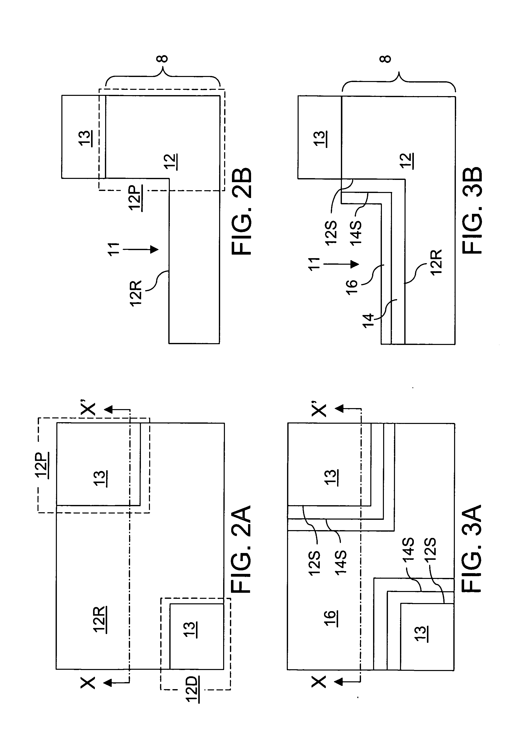
[0064]Referring to FIGS. 2A and 2B, a first exemplary semiconductor structure according to the present invention comprises a semiconductor substrate 8 which includes a p− doped semiconductor layer 12 containing a shallow trench 11. A dielectric pad layer 13 is deposited on a top surface of the semiconductor substrate 8 and is lithographically patterned. The pattern in the dielectric pad layer 13 is transferred into the p− doped semiconductor layer 12 to form the shallow trench 11. The dielectric pad layer 13 comprises a dielectric material such as silicon nitride or silicon oxide. The dielectric pad layer 13 may also comprise a stack of multiple dielectric material layers such as a silicon oxide layer and a silicon nitride layer. The thickness of the dielectric pad layer 13 may be from about 50 nm to about 300 nm, and typically from about 100 nm to about 200 nm, although lesser and greater thicknesses are also contemplated herein. The dielectric pad layer 13 may be formed by low pre...

second embodiment

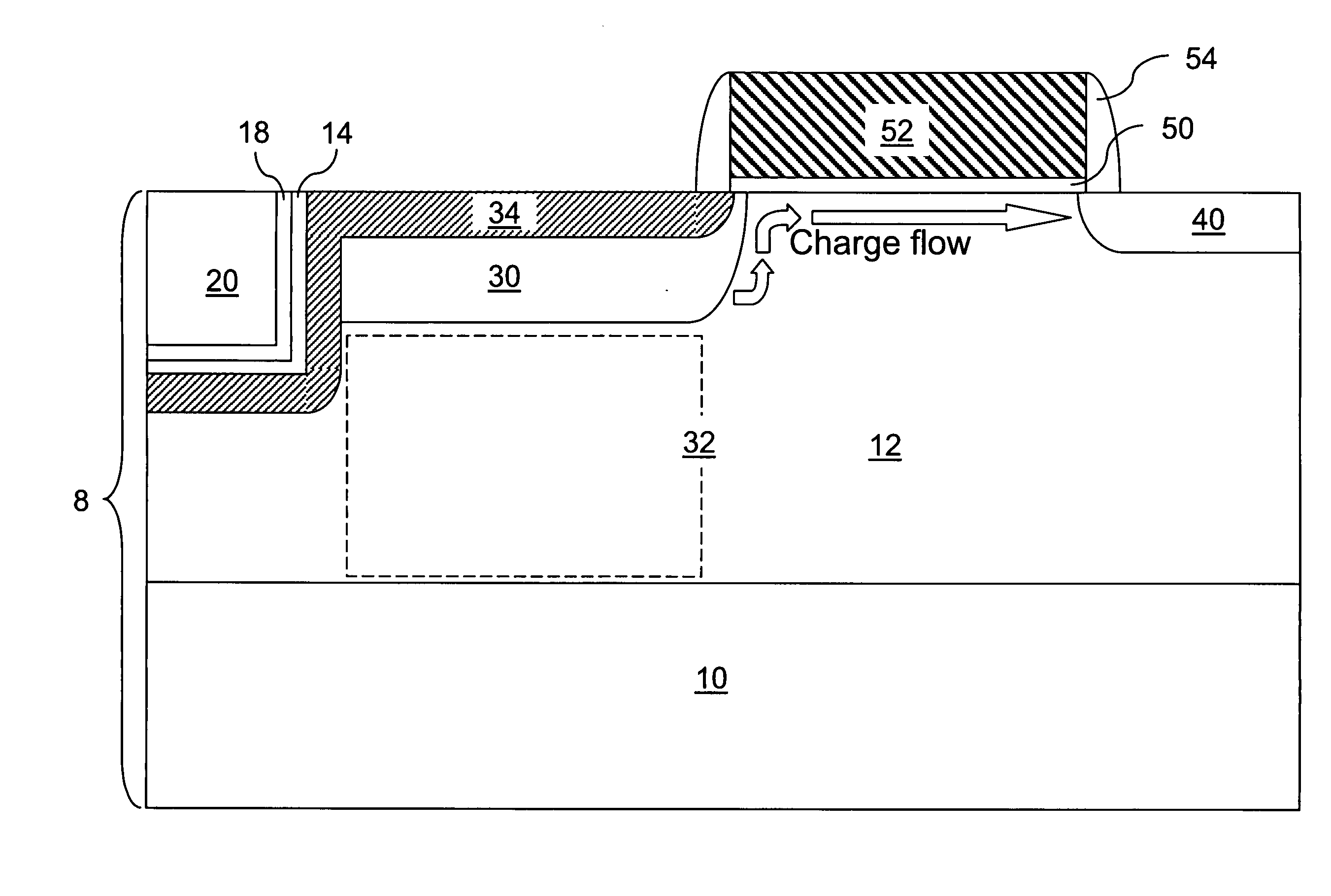
[0077]Referring to FIG. 8, a second exemplary semiconductor structure according to the present invention incorporates the structural and compositional features of the first exemplary semiconductor structure, which include a p− doped semiconductor layer 12, a surface pinning layer 34, a carbon-containing semiconductor layer 14, a dielectric layer 18, and a shallow trench isolation structure 20. The second exemplary semiconductor structure further comprises an n-type charge collection well 30, which is formed directly underneath the surface pinning layer 34 by a masked ion implantation of n-type dopants. The dopant concentration of the n-type charge collection well 30 may be from about 1.0×10¹⁶ / cm3 to about 1.0×10²¹ / cm3, and typically from about 1.0×10¹⁷ / cm3 to about 1.0×10¹⁹ / cm3, although lesser and greater dopant concentrations are explicitly contemplated herein also. The p− doped semiconductor layer 12 includes a p-type well 32 located directly beneath the n-type charge collection ...

fifth embodiment

[0096]Referring to FIG. 19, a fifth exemplary semiconductor structure according to the present invention incorporates the structural and compositional features of the fourth exemplary semiconductor structure, which include a p− doped semiconductor layer 12, a surface pinning layer 34, a carbon-containing semiconductor layer 15, a dielectric layer 18, and a shallow trench isolation structure 20. The second exemplary semiconductor structure further comprises an n-type charge collection well 30, which is formed directly underneath the surface pinning layer 34 by a masked ion implantation of n-type dopants. The dopant concentration of the n-type charge collection well 30 may be from about 1.0×10¹⁶ / cm3 to about 1.0×10²⁰ / cm3, and typically from about 1.0×10¹⁷ / cm3 to about 1.0×10¹⁹ / cm3, although lesser and greater dopant concentrations are explicitly contemplated herein also. The p− doped semiconductor layer 12 includes a p-type well 32 located directly beneath the n-type charge collection...


PUM


Abstract

A carbon-containing semiconductor layer is formed on exposed surfaces of a p-doped semiconductor layer abutting sidewalls of a shallow trench. Following formation of a dielectric layer on the carbon-containing semiconductor layer, a surface pinning layer having a p-type doping is formed underneath the carbon-containing semiconductor layer. A shallow trench isolation structure and a photodiode are subsequently formed. Diffusion of defects directly beneath the shallow trench isolation structure, now contained in the carbon-containing semiconductor layer, is suppressed. Further, boron diffusion into the shallow trench isolation structure and into the photodiode is also suppressed by the carbon-containing semiconductor layer, providing reduction in dark current and enhancement of performance of the photodiode.

Description

FIELD OF THE INVENTION[0001]The present invention relates to a semiconductor structure, and particularly to a complementary metal oxide semiconductor (CMOS) image sensor structure formed on a semiconductor substrate containing a silicon-carbon layer abutting sidewalls and bottom surfaces of a shallow trench isolation structure, and methods of manufacturing the same.BACKGROUND OF THE INVENTION[0002]An image sensor converts a visual image to digital data that may be represented by a picture. The image sensor comprises an array of pixels, which are unit devices for the conversion of the visual image into the digital data. Digital cameras and optical imaging devices employ an image sensor. Image sensors include charge-coupled devices (CCDs) or complementary metal oxide semiconductor (CMOS) image sensors.[0003]While CMOS image sensors have been more recently developed compared to the CCDs, CMOS image sensors provide an advantage of lower power consumption, smaller size, and faster data p...

Claims


Application Information

Patent Timeline
Patent Type & Authority Applications(United States)
IPC IPC(8): H01L31/113H01L31/18
CPCH01L27/14603Y02E10/547
Inventor ADKISSON, JAMES W.KRISHNASAMY, RAJENDRAN
Owner GLOBALFOUNDRIES US INC
Why Eureka
Try Eureka