

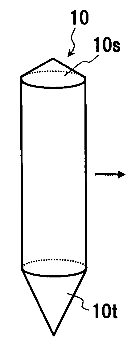
Method of manufacturing polycrystalline silicon rod
a manufacturing method and polycrystalline silicon technology, applied in the direction of polycrystalline material growth, crystal growth process, silicon compounds, etc., can solve the problems of deterioration of the quality (purity) of single-crystalline silicon to be grown, deviation from the initial specified resistivity, and limitations of conventional manufacturing methods of polycrystalline silicon rods, etc., to achieve low impurity contamination, high single-crystallization efficiency, and high purity
- Summary
- Abstract
- Description
- Claims
- Application Information
AI Technical Summary
Benefits of technology
Problems solved by technology
Method used
Image

Examples
example 1
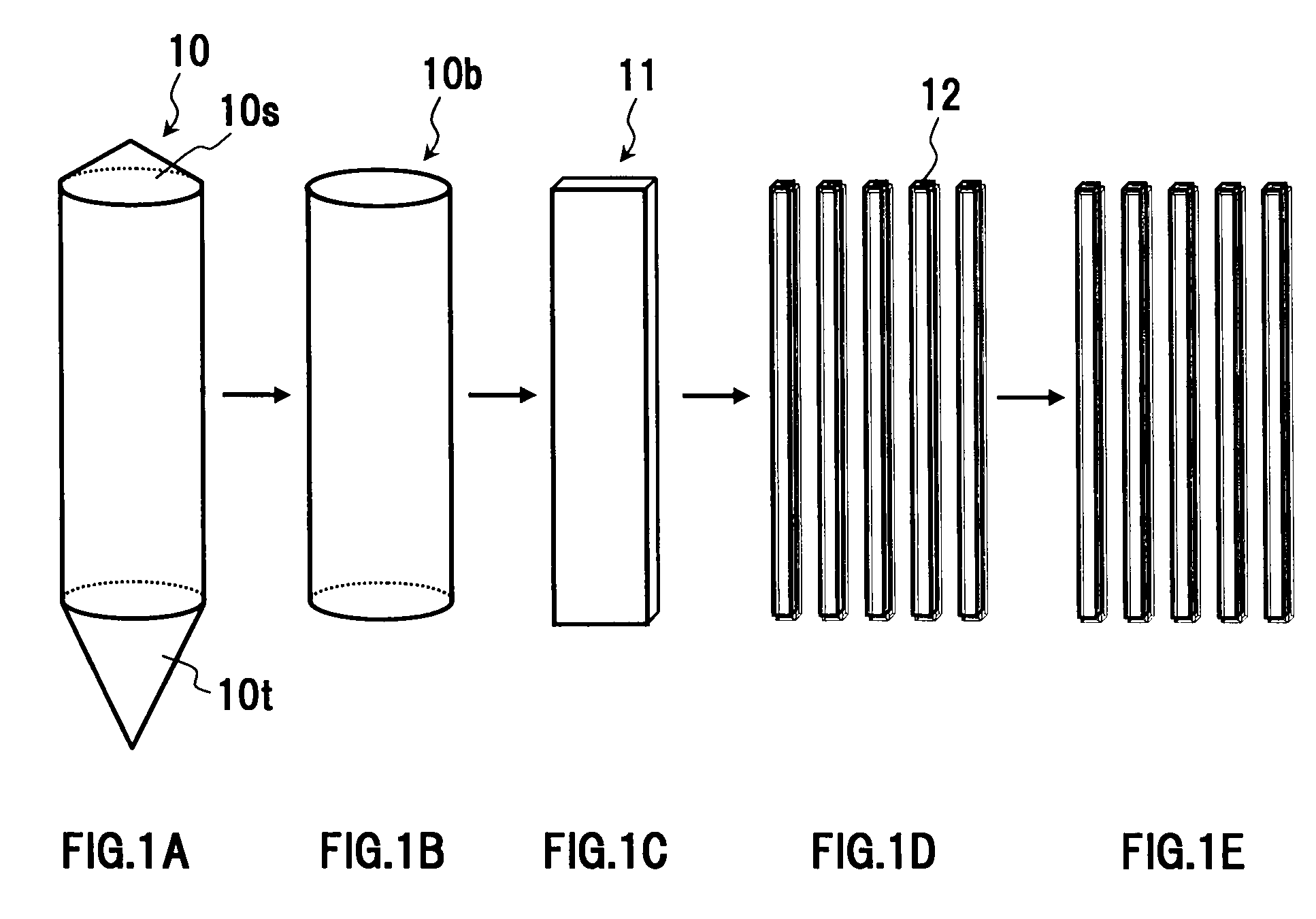
[0047]A single-crystalline silicon, of which crystal growth axis orientation is and which is non-doped (containing no dopant such as P and B), was pulled up by a CZ method. The interstitial oxygen concentration ([Oi]) of the silicon was measured by Fourier transform infrared spectroscopy, and it was revealed that [Oi] is largely constant with respect to the crystal growth axis direction and is within the range of 18.0±1 ppma (the conversion factor fc=6.06; see T. Iizuka, S. Takasu, M. Tajima, T. Arai, M. Nozaki, N. Inoue and M. Watanabe “Conversion coefficient of IR measurement of oxygen in Si”, Defects in Silicon, pp. 265-274, Electrochem. Society (1983)).
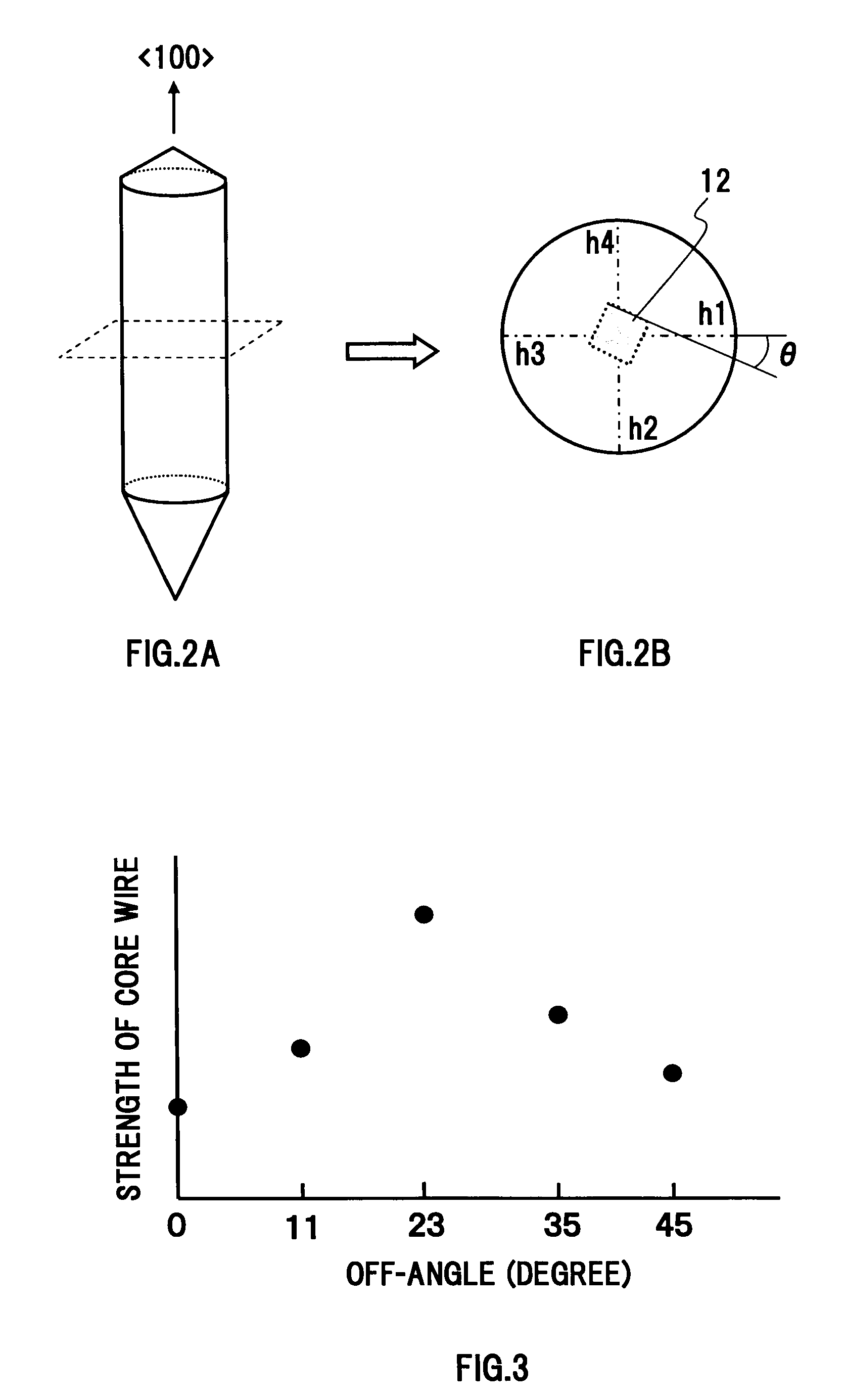
[0048]A planar silicon having a thickness of 7 mm in the growth axis direction was cut out with an off-angle (0, 11, 23, 35, 45 degrees) with reference to the crystal habit line which appears in the crystal growth axis direction of the single-crystalline silicon, and the planar silicon was further cut into thin rectangles with a ...
example 2
[0050]An attempt was made to manufacture a polycrystalline silicon rod by using a single-crystalline silicon core wire (with an off-angle of 23 degrees) fabricated by the method according to the above described in Example 1.
[0051]FIG. 4 summarizes the core-wire breakage rate during a CVD process with and without an off-angle. It is seen that providing an off-angle decreases the core-wire breakage rate by not less than one order of magnitude.
example 3
[0052]In the present example as well, a polycrystalline silicon rod was fabricated using a single-crystalline silicon core wire (with an off-angle 23 degrees) fabricated by a similar method as that of Example 1, and this polycrystalline silicon rod was used to grow a single-crystalline silicon by an FZ method. Moreover, for the purpose of comparison, a single-crystalline silicon was fabricated by an FZ method using a polycrystalline silicon rod which was grown using a conventionally known polycrystalline silicon core wire.
[0053]FIG. 5 shows the comparison of an FZ success rate of the polycrystalline silicon rod between the cases in which a polycrystal core wire and a single-crystalline core wire are used respectively. As clearly seen from this figure, use of a polycrystalline silicon rod using a single-crystalline core wire improved the FZ success rate. That is, it is seen that the one-pass rate has been improved.
[0054]As so far described, the present invention provides a method to ...
PUM
| Property | Measurement | Unit |
|---|---|---|
| Length | aaaaa | aaaaa |
| Length | aaaaa | aaaaa |
| Angle | aaaaa | aaaaa |
Abstract
Description
Claims
Application Information