Photovoltaic Structures and Method to Produce the Same

a photovoltaic and structure technology, applied in the field of organic optoelectronics, can solve the problem of difficult to achieve a very fine phase separation between the electron donor material and the donor material

Inactive Publication Date: 2009-12-17
INTERUNIVERSITAIR MICRO ELECTRONICS CENT (IMEC VZW)
View PDF5 Cites 32 Cited by
  • Summary
  • Abstract
  • Description
  • Claims
  • Application Information

AI Technical Summary

Problems solved by technology

The major bottleneck for achieving highly efficient organic solar cells is balancing the low diffusion length (LD) inherent to current organic semiconductors while achieving sufficiently thick layers to absorb most of the incident light.
However, it is diffic

Method used


Image

  • Photovoltaic Structures and Method to Produce the Same
  • Photovoltaic Structures and Method to Produce the Same
  • Photovoltaic Structures and Method to Produce the Same

Examples


example 1

Investigation of the Usability in Embodiments of the Present Embodiment of a SY:PtOEP host:guest System in a Donor Material

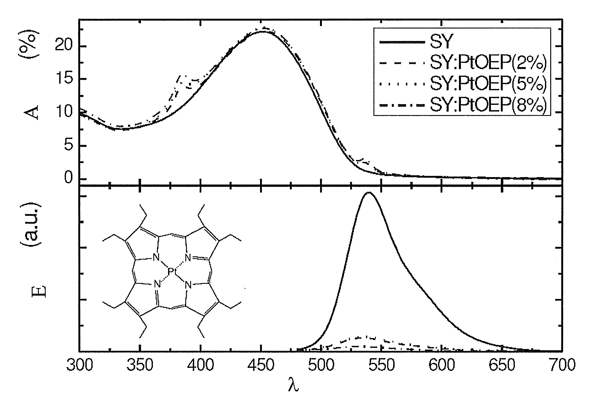
[0189]As an example the phenyl-substituted poly(p-phenylene vinylene) (PPV) donor polymer Super Yellow (SY) obtainable from Merck OLED materials GmbH (see formula (I)) doped with the phosphorescent molecule platinum octaethylporphyrin (PtOEP) (see formula II) is used.

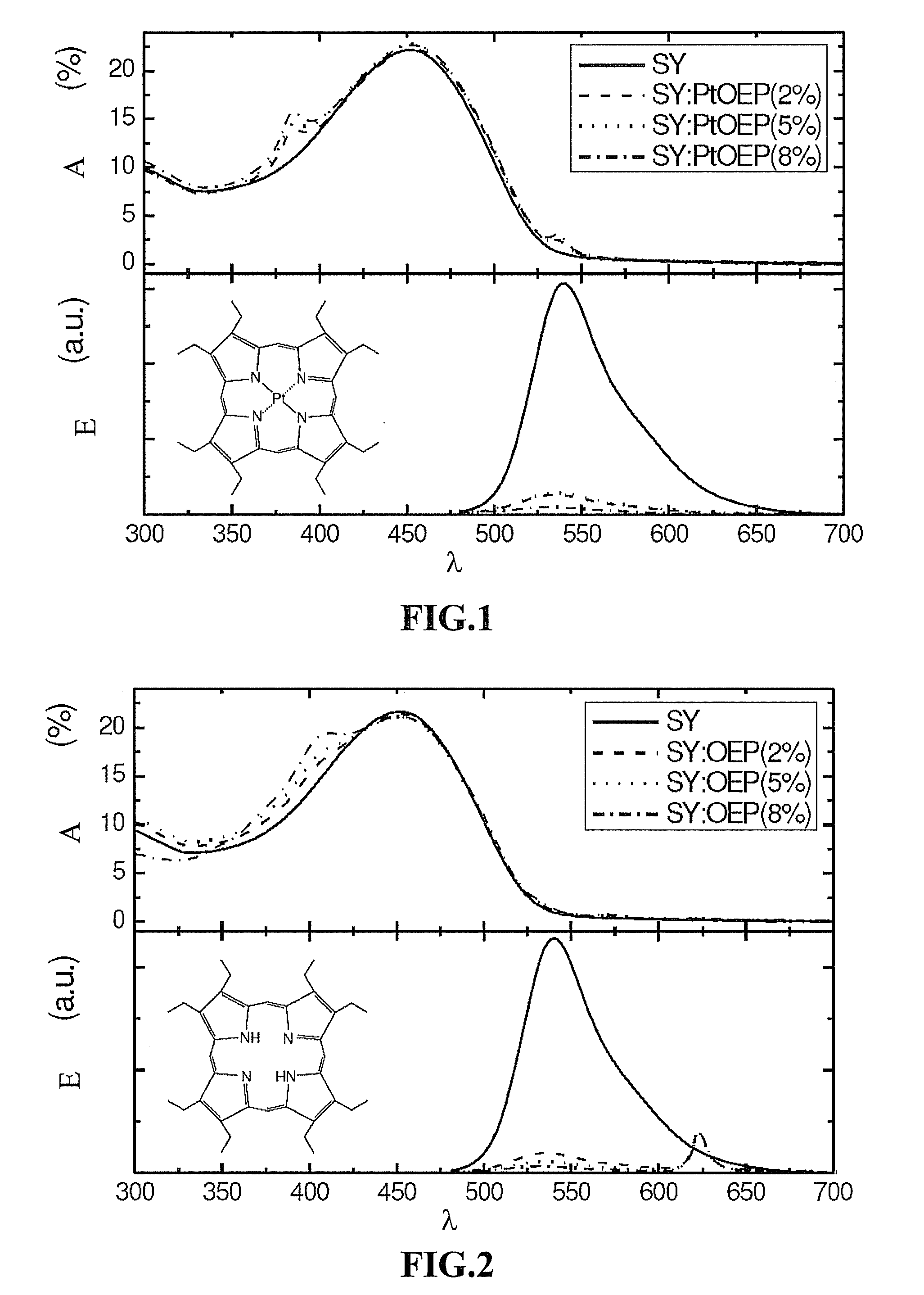
[0190]Furthermore, the effect of doping with the Pt-free analogue of (II) octaethylporphyrin (OEP) (III) was investigated to demonstrate the opposite effect: a dopant that allows singlet energy transfer (SET) but not triplet energy transfer (TET) is expected to actually reduce the photocurrent.

[0191]FIG. 1 shows the absorption and emission of a pure SY (I) film as well as films doped with PtOEP (II), whereas FIG. 2 shows SY (I) films doped with OEP. The absorption shoulders of PtOEP (II) and OEP (III) are present in the doped films, at wavelengths of λ=385 and 535 nm for PtOEP (II) and at λ=410 nm f...

example 2

Investigation of the Usability in Embodiments of the Present Embodiment of a MEH-PPV:PtOEP host:guest System in a Donor Material

[0192]FIG. 5 shows the absorption and emission of a pure MEH-PPV (VI) film (curves A and A′ respectively) as well as films doped with PtOEP (II) (curves B and B′ respectively). The absorption shoulder of PtOEP (II) is present in the doped films, at the wavelength of λ=385 nm. The MEH-PPV (VI) emission, with its peak at λ=562 nm, is quenched as a result of the introduction of the guest PtOEP (II). Indeed, as shown in FIG. 5, the MEH-PPV (VI) emission is decreased to about 12% of its initial value upon the addition of 5% PtOEP (II) in the polymer matrix. Perhaps most importantly, however, is that PtOEP (II) phosphorescence at λ=650 nm is not present. This suggests a similar excitonic pathway to that illustrated schematically in FIG. 4, where for the case of PtOEP (II) there is efficient SET from MEH-PPV (VI) to PtOEP (II) molecules, followed by ISC, and final...

example 3

Investigation of the Usability in Embodiments of the Present Embodiment of a MDMO-PPV:PtOEP host:guest System

[0193]FIG. 6 shows the absorption and emission of a pure MDMO-PPV (V) film (curves C and C′ respectively) as well as films doped with PtOEP (II) (curves D and D′ respectively). The absorption shoulder of PtOEP (II) is present in the doped films, at the wavelength of λ=385 nm. The MDMO-PPV (VI) emission, with its peak at λ=567 nm, is quenched as a result of the introduction of the guest PtOEP (II). Indeed, as shown in FIG. 6, the MDMO-PPV (VI) emission is decreased to about 32% of its initial value upon the addition of 5% PtOEP (II) in the polymer matrix. Perhaps most importantly, however, is that PtOEP (II) phosphorescence at λ=650 nm is not present. This suggests a similar excitonic pathway to that illustrated schematically in FIG. 4, where for the case of PtOEP (II) there is efficient SET from MDMO-PPV (VI) to PtOEP (II) molecules, followed by ISC, and finally TET back to M...


PUM

PropertyMeasurementUnit
Molar massaaaaaaaaaa
Weight ratioaaaaaaaaaa
Structureaaaaaaaaaa

Abstract

The present disclosure relates to the field of organic optoelectronics. More particularly, the present disclosure relates to photovoltaic structures and to methods to produce the same. One aspect of the disclosure is a photovoltaic structure comprising:
    • an electron acceptor material, and
    • an electron donor material, wherein the electron donor material comprises:
      • a host material, and
      • a guest material,
wherein the energy of the lowest excited singlet state of the guest is smaller than the energy of lowest excited singlet state of the host, wherein the fluorescence emission spectrum of the host overlaps with at least part of the absorption spectrum of the guest and wherein the energy of the lowest excited triplet state of the guest is larger than the energy of the lowest excited triplet state of the host.

Description

CROSS-REFERENCE TO RELATED APPLICATIONS[0001]This application claims priority to U.S. Provisional Application Ser. No. 60 / 061,451 filed Jun. 13, 2008 and European Patent Application Serial No. 08167746.0 filed Oct. 28, 2008, the contents of each of which are incorporated by reference herein in its entirety.TECHNICAL FIELD OF THE INVENTION[0002]The present invention relates to the field of organic optoelectronics. More particularly, the present invention relates to photovoltaic structures and to methods to produce the same.BACKGROUND OF THE INVENTION[0003]Recently, the power conversion efficiency of organic photovoltaics has improved rapidly, offering new potential as low-cost renewable energy sources, driven primarily by the development of new materials, device architectures, and processing techniques. Since the absorption of a photon in an organic semiconductor results in the creation of a bound electron-hole pair, also called an exciton, the device performance relies on the abilit...

Claims


Application Information

Patent Timeline
IPC IPC(8): H01L51/46H01L51/48
CPCH01L51/0038Y02E10/549H01L51/424H01L51/0087H10K85/114H10K85/346H10K30/20
Inventor RAND, BARRYGENOE, JANHEREMANS, PAUL
Owner INTERUNIVERSITAIR MICRO ELECTRONICS CENT (IMEC VZW)
Why Eureka
Try Eureka