
Atomic layer deposition for functionalizing colloidal and semiconductor particles

a technology of atomic layer and colloidal particles, which is applied in the direction of semiconductor devices, electrical apparatus, nanotechnology, etc., can solve the problems of achieve the effect of efficient functionalizing useful electronic components, improving electronic coupling, and high resistivity limits device application

Active Publication Date: 2009-12-24
UCHICAGO ARGONNE LLC
View PDF2 Cites 22 Cited by
  • Summary
  • Abstract
  • Description
  • Claims
  • Application Information

AI Technical Summary

Benefits of technology

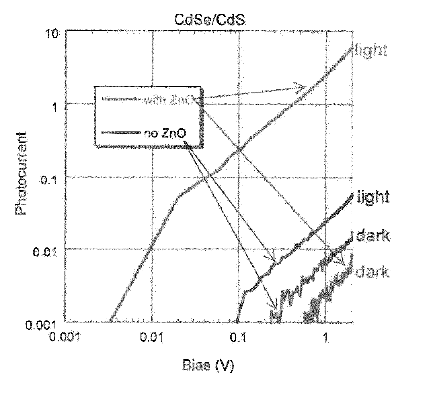
[0008]In order to efficiently functionalize useful electronic components from colloidal nanoparticle systems, organic layers conventionally used to coat and passivate the starting nanoparticles are replaced with ALD layers of various inorganic materials. The organic layers present a significant barrier to the flow of electrical charge and the resulting high resistivity limits device application. Replacement of the organic layer with a lower electronic barrier material, such as an inorganic semiconductor, leads to greatly improved electronic coupling between the colloidal nanoparticles, enabling a wide variety of electronic, optical and chemical applications, such as photovoltaics, solid state lighting and electrically driven lasers. A preferred method of preparation involves liquid phase deposition of solid colored colloidal quantum dot arrays followed by gas phase ALD of a selected inorganic barrier layer.
[0010]In an another embodiment, a functionalized nanocomposite that has enhanced electro-optical properties is described. The nanocomposite comprises a semiconductor nanocrystal substrate and an inorganic conformal film deposited over at least a portion of the substrate via monolayer deposition. The inorganic film comprises a transition metal and the nanocomposite is characterized by an enhancement of at least one of an electrical property and an optical property relative to the respective electrical property and optical property of the semiconductor nanocrystal.

Problems solved by technology

The organic layers present a significant barrier to the flow of electrical charge and the resulting high resistivity limits device application.

Method used


Image

  • Atomic layer deposition for functionalizing colloidal and semiconductor particles
  • Atomic layer deposition for functionalizing colloidal and semiconductor particles
  • Atomic layer deposition for functionalizing colloidal and semiconductor particles

Examples


example 1

[0041]The colloidal dots and core / shells are synthesized following slight modifications of a conventional procedure (see FIG. 8). As synthesized, the dot solutions have a large excess of non-volatile hydrocarbons. These hydrocarbons are first cleaned off by an initial precipitation and centrifugation with ethanol. The dots are then further cleaned by re-dissolving the precipitate in CCl4, with 0.2 vol % tri-n-octylphosphine (TOP) and tri-n-octylphosphine oxide (TOPO) dissolved, followed by centrifugation, transfer of the clear quantum dot solution to a clean test-tube and precipitation with ethanol by centrifugation. This is repeated twice. Finally, the precipitate is dried and redissolved in a mixture of hexane and octane (9:1). This solution is then centrifuged and filtered. Drop-casting leads to clear dry films between 50 and 80 nm thick and an optical density of 0.01 to 0.05 at the exciton peak (the smaller value is for core / shells).

[0042]Such films are highly insulating and exh...

example 2

[0043]In a preferred method of Example 1, a solution of tri-n-octylphosphine oxide (TOPO) at 300° C. is prepared. A solution of Cd and Se precursors (e.g. (CH3)3Cd+(CH3)3Se in tri-n-octylphosphine (TOP) is prepared, and this solution is injected into the last TOPO solution. First nucleation of CdSe is obtained by thermal decomposition. The system is rapidly cooled to about 260° C. and the slow growth of CdSe quantum dots ensues. The size of the quantum dot is determined by the duration of the growth step. Specific examples are described hereinafter.

example 3

[0044]Measurements were carried out to determine photoluminescence (PL) under 354 nm UV lamp irradiation following ALD of Al2O3 on various CdSe / CdS and CdSe quantum dots prepared in the manner described in Examples 1 and 2. As noted in FIGS. 9A-9D, various ALD temperatures were used and selected samples were subject to an NH4OH dip. Of note, is the effect of these parameters on the photoluminescence of the various specimens, and in particular, that higher ALD growth temperatures quench the photoluminescence.


PUM

PropertyMeasurementUnit
energy barriersaaaaaaaaaa
coupling energyaaaaaaaaaa
thicknessaaaaaaaaaa

Abstract

A method for producing a product of a functionalized nanocomposition colloidal material using atomic layer deposition to coat the colloidal material. The ALD layer comprises an inorganic material which enables improved optical and electrical properties for the nanocomposite.

Description

CROSS REFERENCE TO RELATED PATENT APPLICATIONS[0001]The present application claims priority to U.S. Provisional Patent Application No. 61 / 073,286, filed Jun. 17, 2008, and incorporated herein by reference in its entirety.STATEMENT OF GOVERNMENT INTEREST[0002]The United States Government claims certain rights in this invention pursuant to Contract No. W-31-109-ENG-38 between the United States Government and the University of Chicago and / or pursuant to DE-AC02-06CH11357 between the United States Government and UChicago Argonne, LLC representing Argonne National Laboratory.FIELD OF THE INVENTION[0003]This invention is directed to functionalizing nano-particles using atomic layer deposition (ALD) for a variety of electronic applications. More particularly, the invention is directed to preparation of functionalized nanocomposites of colloidal quantum dots having a deposited layer formed by ALD. A selected film layer can be deposited by ALD to improve electronic properties of the colloida...

Claims


Application Information

Patent Timeline
Patent Type & Authority Applications(United States)
IPC IPC(8): H01L29/66H01L21/205
CPCB82Y10/00H01L21/02554H01L21/02557H01L29/225H01L21/0262H01L29/22H01L29/2203H01L21/0256
Inventor ELAM, JEFFREY W.GUYOT-SIONNEST, PHILIPPE
Owner UCHICAGO ARGONNE LLC
Learn More