Optical information recording medium and method for manufacturing the same

Inactive Publication Date: 2010-02-25
PANASONIC CORP
26 Cites 8 Cited by

AI-Extracted Technical Summary

Problems solved by technology

However, TiO2, which has been used conventionally as a material for the transmittance adjusting layer, has problems in that it takes a longer time to manufacture an information recording medium since it has a low deposition rate during sputtering and a great variation in deposition rate due to moisture, and it is difficult to maintain a constan...

Method used

[0021]In each of the first optical information recording medium and the second optical information recording medium of the present invention, the transmittance adjusting layer preferably has a thickness of at least 3 nm but not more than 40 nm, or at least 60 nm but not more than 130 nm. Thereby, the transmittance of the information layer including the transmittance adjusting layer can be enhanced.
[0028]The second information layer 20 includes a second lower protective layer 12, a second lower interface layer 13, a second recording layer 14, a second upper interface layer 15, a second upper protective layer 16, a second reflective layer 17, and a first substrate 18 disposed sequentially from the laser beam 30 incident side. In the names of the interface layers and the protective layers in this specification, “lower” means that the layer is disposed on the laser beam 30 incident side with respect to the recording layer, and “upper” means that the layer is disposed on a side opposite to the laser beam 30 incident side with respect to the recording layer. Furthermore, when a plurality of layers having similar functions are provided in the optical information recording medium 100 of the present embodiment, they are differentiated from each other by being referred to as a first, a second, sequentially from the laser beam 30 incident side for easier explanation.
[0031]Guide grooves for guiding the laser beam 30 may be formed on an inner surface (on an optical separation layer 21 side) of the first substrate 18, if needed. An outer surface of the first substrate 18 preferably is smooth. Preferably, the first substrate 18 has low optical birefringence in a short wavelength region. As the material for the first substrate 18, polycarbonate particularly is preferable because it has excellent transferability and mass productivity, and is inexpensive. The cover layer 1 has a thickness in a range of, for example, 10 μm to 800 μm (preferably 50 μm to 150 μm, or 550 μm to 650 μm). The first substrate 18 has a thickness in a range of, for example, 400 μm to 1300 μm (preferably 550 μm to 650 μm, or 1050 μm to 1150 μm).
[0032]The first lower protective layer 2, the first upper protective layer 5, the second lower protective layer 12, and the second upper protective layer 16 each are formed of a dielectric material. These protective layers have a function of adjusting the optical distance to increase the optical absorption efficiencies of the recording layers and a function of increasing the change in amount of reflected light between before and after recording to increase the signal amplitude. Examples of the material that can be used for these protective layers include oxides such as SiOx (x is 0.5 to 2.5), Al2O3, TiO2, Ta2O5, ZrO2, ZnO, Cr2O3, Ta2O5, Bi2O3, Bi4T3O12, CeO2, Cu2O, In2O3, MgO, MgSiO3, Nb2O5, SnO2, WO3, Y2O3, ZrSiO4, and Te—O. Nitrides such as Si—N, Al—N, Ti—N, Ta—N, Zr—N, and Ge—N also can be used. Furthermore, sulfides such as ZnS and carbides such as SiC also can be used. In addition, a mixture of the above-mentioned materials also can be used.
[0033]The thicknesses of the first lower protective layer 2 and the first upper protective layer 5 can be determined precisely so that the change in amount of reflected light is large between the case where the first recording layer 4 is in a crystalline phase and the case where it is in an amorphous phase, the first information layer 10 has a high transmittance, and the first recording layer 4 has a high optical absorption efficiency. Specifically, these thicknesses can be determined using, for example, a calculation based on a matrix method.
[0035]Similarly, the thicknesses of the second lower protective layer 12 and the second upper protective layer 16 also can be determined precisely so that the change in amount of reflected light is large between the case where the second recording layer 14 is in a crystalline phase and the case where it is in an amorphous phase, and the second recording layer 14 has a high optical absorption efficiency.
[0039]For the first upper protective layer 5 and the second upper protective layer 16, an oxide material preferably is used in order to prevent mass transfer from occurring due to repetitive recording. Preferably, a material obtained by mixing ZrO2, SiO2, and Cr2O3 is used, for example.
[0044]Preferably, the thickness of the first recording layer 4 is 9 nm or less, and more preferably, in a range of 5 nm to 7 nm, in order to increase the transmittance of the first information layer 10 so that a necessary amount of laser beam for recording and reproducing information on and from the second information layer 20 reach the second information layer 20.
[0045]Preferably, the thickness of the second recording layer 14 is in a range of 6 nm to 15 nm in order to increase the recording sensitivity of the second information layer 20. Preferably, the thickness of the second recording layer 14 is in a range of 8 nm to 12 nm, taking into account the thermal effect on an adjacent region (a region adjacent to the region on which recording is performed under laser beam irradiation) caused by the in-plane heat diffusion that occurs when the second recording layer14 is thick, and the decrease in reflectance of the second information layer 20 that occurs when the second recording layer 14 is thin.
[0047]The first reflective layer 6 and the second reflective layer 17 each have an optical function of increasing the amount of light to be absorbed by the first recording layer 4 and the second recording layer 14, respectively. These reflective layers also have a thermal function of diffusing quickly the heat generated in the recording layers (the first recording layer 4 and the second recording layer 14) so as to facilitate the amorphization of the recording layers. Furthermore, these reflective layers also have a function of protecting a multilayer film constituting the optical information recording medium 100 from the environment in which it is used.
[0048]As the material for the first reflective layer 6 and the second reflective layer 17, a single metal with a high thermal conductivity, such as Al, Au, Ag, and Cu, can be used. Or it is possible to use an alloy containing, as a main component, one or more elements selected from these metal elements and one or more other elements that are added thereto in order to, for example, enhance the moisture resistance and adjust the thermal conductivity. Specifically, an alloy such as Al—Cr, Al—Ti, Au—Pd, Au—Cr, Ag—Pd, Ag—Pd—Cu, Ag—Pd—Ti, Ag—Ru—Au, and Cu—Si can be used. These alloys are all excellent materials having excellent corrosion resistance and satisfying rapid cooling requirements. Particularly, an Ag alloy is preferable as the material for the first reflective layer 6 because it has a high thermal conductivity and also a high light transmittance.
[0049]Preferably, the first reflective layer 6 has refractive index n2 and extinction coefficient k2 that satisfy n2≦2.0 and 1.0≦k2, respectively in order to increase further the transmittance of the first information layer 10. More preferably, they satisfy 0.1≦n2≦1.0 and 1.5≦k2≦4.0, respectively.
[0050]In order to increase the transmittance Tc (%) and transmittance Ta (%) of the first information layer 10 as much as possible, the thickness of the first reflective layer 6 preferably is in a range of 5 nm to 15 nm, and more preferably in a range of 8 nm to 12 nm. When the thickness of the first reflective layer 6 is less than 5 nm, the thermal diffusion function thereof may be insufficient and the reflectance of the first information layer 10 may be lowered. When the thickness of the first reflective layer 6 is more than 15 nm, the transmittance of the first information layer 10 may be insufficient. In this specification, the transmittance Tc (%) represents the transmittance of the first infor...

Benefits of technology

[0015]According to the optical information recording medium of the present invention and the method for manufacturing the optical information recording medium, it is possible to form the transmittance adjusting layer at a stably high deposition rate, and to increase...

Abstract

An optical information recording medium of the present invention includes at least a recording layer (4) that allows information to be recorded thereon and/or reproduced therefrom by being irradiated with a laser beam, and a transmittance adjusting layer (7) in this order from an incident side of the laser beam (30). In the optical information recording medium of the present invention, the transmittance adjusting layer (7) contains Bi, Ti, and O and with a composition of Bi, Ti, and O contained in the transmittance adjusting layer (7) being denoted as BixTiyOz, in atomic number ratio, x, y, and z satisfy 0.07≦x≦0.35, 0.07≦y≦0.28, 0.56≦z≦0.70, and x+y+z=1. Or the transmittance adjusting layer (7) contains Bi2O3 and TiO2, and with a composition of Bi2O3 and TiO2 contained in the transmittance adjusting layer (7) being denoted as (Bi2O3)α(TiO2)β, in molar ratio, α and β satisfy 0.2≦α≦0.7, 0.3≦β≦0.8, and α+β=1

Application Domain

Layered productsVacuum evaporation coating +8

Technology Topic

TransmittanceLaser beams +2

Image

  • Optical information recording medium and method for manufacturing the same
  • Optical information recording medium and method for manufacturing the same

Examples

  • Experimental program(26)

Example

EXAMPLE
[0084]Hereinafter, the optical information recording medium of the present invention will be described in further detail with reference to examples.

Example

Example 1
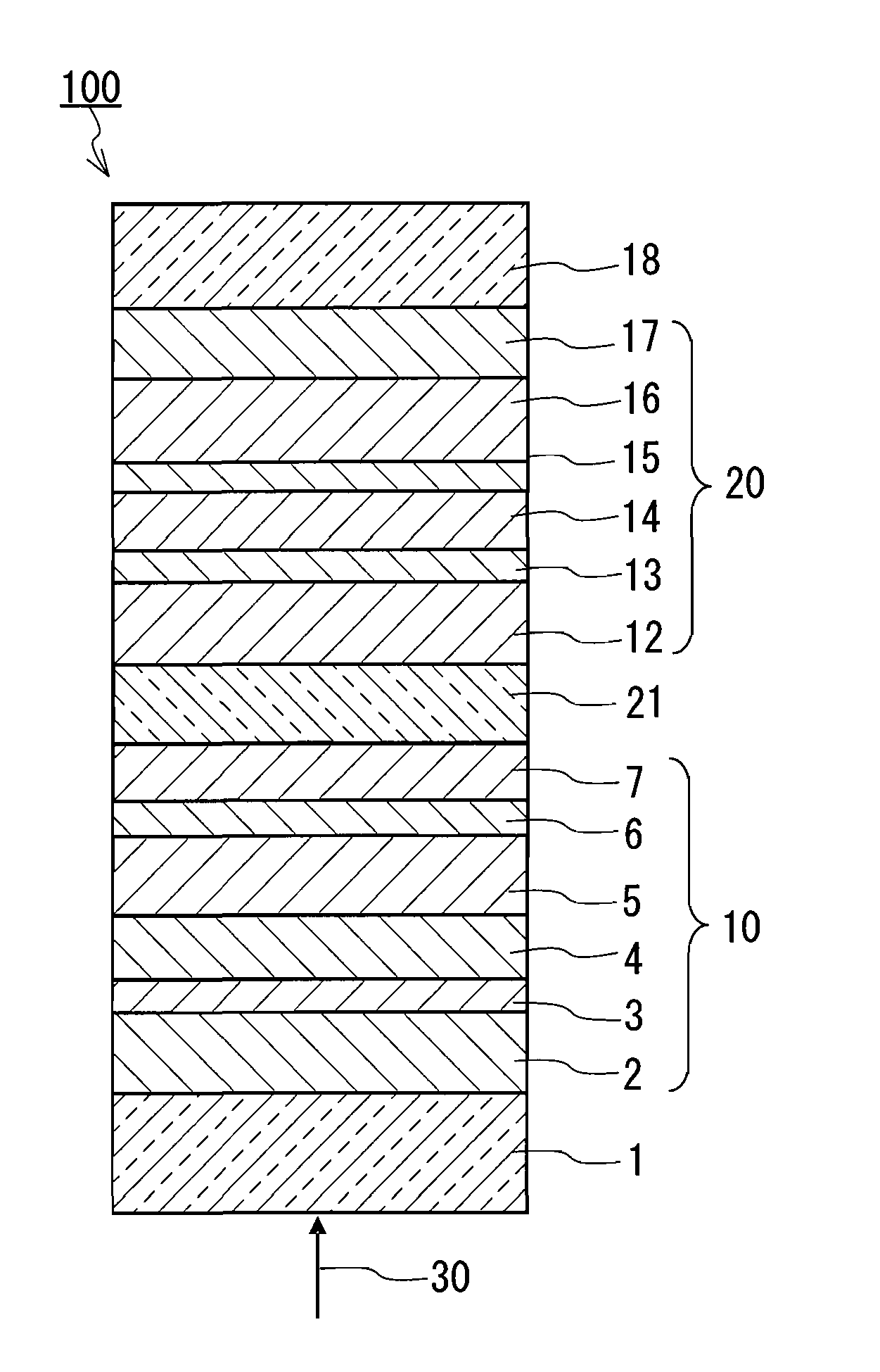
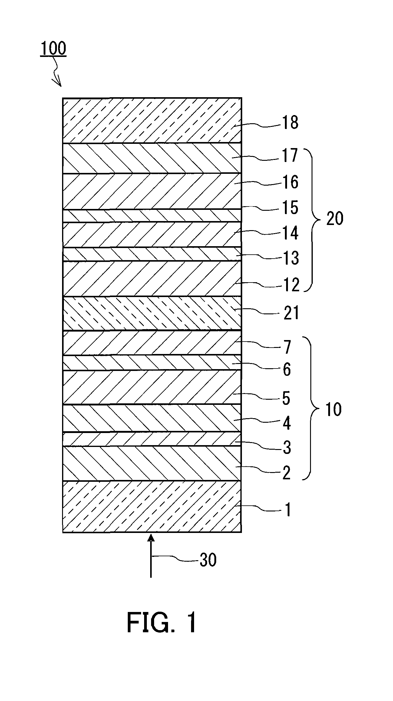
[0085]The optical information recording medium of Example 1 was produced as follows. The optical information recording medium produced in the present example had the same film structure as that of the optical information recording medium 100 shown in FIG. 1, except that the first upper interface layer was provided further between the first recording layer 4 and the first upper protective layer 5. The optical information recording medium of the present example will be described below using the numerals shown in FIG. 1.
[0086]First, a 1.1 mm-thick polycarbonate substrate (120 mm in diameter and 1100 μm in thickness) with guide grooves transferred thereon was used as the first substrate 18.
[0087]Then, the second information layer 20 was formed on the polycarbonate substrate by stacking sequentially an Ag—Pd—Cu layer (100 nm in thickness) as the second reflective layer 17, a ZrO2—Cr2O3 layer (12 nm in thickness) as the second upper protective layer 16, a ZrO2—SiO2—Cr2O3 layer (2 nm in thickness) as the second upper interface layer 15, an Sb80Ge7Te13 layer (10 nm in thickness) as the second recording layer 14, a ZrO2—SiO2—Cr2O3 layer (5 nm in thickness) as the second lower interface layer 13, and a ZnS—SiO2 layer (40 nm in thickness, ZnS 80 mol % and SiO2 20 mol %) as the second lower protective layer 12, by a sputtering method.
[0088]Next, in order to form the optical separation layer 21, the ultraviolet curable resin was applied on the second lower protective layer 12 by a spin coat method, the substrate (mold) with grooves was placed on the resin that had not been cured yet, and then the resin was cured. Subsequently, the substrate (mold) was separated therefrom. Thus, the optical separation layer 21 with the guide grooves was formed.
[0089]Next, the medium with the optical separation layer 21 was placed in an oven maintained at a temperature of 80° C. and a relative humidity of 1% for 4 hours, and then the medium was placed in a vacuum device. Thereafter, each of the films constituting the first information layer 10 was formed by sputtering.
[0090]The first information layer 10 was formed by stacking sequentially the transmittance adjusting layer 7 (14 nm to 25 nm in thickness), an Ag—Pd—Cu layer (10 nm in thickness) as the first reflective layer 6, a ZrO2—Cr2O3 layer (12 nm in thickness) as the first upper protective layer 5, a ZrO2—SiO2—Cr2O3 layer (2 nm in thickness) as the first upper interface layer, a Ge12Bi2Te15 layer (7 nm in thickness) as the first recording layer 4, a ZrO2—Cr2O3 layer (5 nm in thickness) as the first lower interface layer 3, and a ZnS—SiO2 layer (45 nm in thickness, ZnS 80 mol % and SiO2 20 mol %) as the first lower protective layer 2. Finally, the ultraviolet curable resin was applied on the first lower protective layer 2, a polycarbonate substrate (120 mm in diameter and 90 μm in thickness) was placed on the first lower protective layer 2 and subject to spin coating, and then it was irradiated with an ultraviolet ray to cure the resin. Thus, the cover layer 1 (75 μm in thickness) was formed.
[0091]The first reflective layer 6 and the second reflective layer 17 were formed using an Ag97Pd2Cu1 (wt %) material (a mixture of 97 wt % of Ag, 2 wt % of Pd, and 1 wt % of Cu), by DC sputtering and with an Ar gas introduced.
[0092]The second upper protective layer 15, the first upper protective layer 5, and the first lower interface layer 3 were formed using a (ZrO2)50(Cr2O3)50 (mol %) material by RF sputtering with an Ar gas introduced.
[0093]The second upper interface layer 17, the second lower interface layer 13, and the first upper interface layer were formed using a (ZrO2)50(Cr2O3)50 (mol %) material by RF sputtering with an Ar gas introduced.
[0094]The second recording layer 14 was formed using a mixed material of Sb80Ge7Te13 (atom %) by DC sputtering with an Ar gas introduced. “Sb80Ge7Te13 (atom %)” is a composition formula, where the sum total of “Sb” atoms, “Ge” atoms, and “Te” atoms is taken as a reference (100%).
[0095]The first recording layer 4 was formed using a material obtained by mixing GeTe, SnTe, and Bi2Te3 at a molar ratio of 10:2:1, by DC sputtering with an Ar gas introduced.
[0096]The first lower protective layer 2 was formed using a material obtained by mixing ZnS and SiO2 at a molar ratio of 4:1, by RF sputtering with an Ar gas introduced.
[0097]The cover layer 1 was formed using a polyester acrylate material.
[0098]The transmittance adjusting layer 7 of the present example was formed by sputtering, and the size of the sputtering target used was 200 mm in diameter×6 mm in thickness. It was proved that a pulse frequency of 120 Hz and a pulse reverse time of 0.4 μs can stabilize the electrical discharge without lowering the sputtering rate.
[0099]The transmittance adjusting layer 7 was formed to have a thickness of 18 nm, using a sputtering target obtained by mixing 20 mol % of Bi2O3 powder and 80 mol % of TiOx powder (x=1.6 to 1.8) as the sputtering target. In the present example, an electric power of 2.5 kW was used for sputtering. Moreover, magnetron sputtering was used for the sputtering.
[0100]In the present example, a gas containing inexpensive Ar gas as a main component was used, and oxygen gas was introduced in order to accelerate oxidation further when forming the thin film out of the sputtering target. The thin film (the transmittance adjusting layer 7) was formed with Ar gas flow rate being fixed at 3.3×10⁻⁷ m3/s (20 sccm), and with oxygen gas being introduced so that the oxygen concentration during sputtering was 3 vol %. At this time, the degree of vacuum in the film formation room was approximately 2×10⁻¹ Pa.
[0101]In the optical information recording medium of the present example thus produced, the first information layer 10 was evaluated for recording/reproducing characteristics. The evaluation method will be described hereinafter.
[0102]As the recording/reproducing apparatus, a recording/reproducing apparatus including a spindle motor for rotating the optical information recording medium, an optical head having a semiconductor laser, and an objective lens for focusing a laser beam emitted from the semiconductor laser.
[0103]First, common methods for recording, erasing, and overwrite recording with respect to the optical information recording medium will be described. Recording, erasing, and overwrite recording of information with respect to the optical information recording medium can be performed through modulation of the laser beam power between a peak power (Pp (mW)) of high power and a bias power (Pb (mW)) of low power. An amorphous phase is formed in a local area of the recording layer by irradiation with a laser beam of the peak power, and the amorphous phase serves as a mark. The region between the recording marks is irradiated with a laser beam of the bias power and thereby a crystalline phase (an erased area) is formed. In the case of irradiation with a laser beam of the peak power, it is common to employ a so-called multipulse composed of pulse trains. The multipulse may be modulated only at levels of the peak power and the bias power, or may be modulated at a level in a range of 0 mW to the peak power.
[0104]The power used as a reproducing power (Pr (mW)) has a power level lower than those of the peak power and bias power. The laser beam irradiation at the power level of the reproducing power does not affect the optical states of the recording marks, and makes it possible to obtain a sufficient amount of reflected light from the optical information recording medium to reproduce the recording marks. A detector detects the signals from the optical information recording medium, which are obtained by irradiation with the laser beam of the reproducing power. Thus, the information signals are reproduced.
[0105]The numerical aperture NA of the object lens preferably is in a range of 0.5 to 1.1 (more preferably in a range of 0.6 to 1.0) in order to adjust the spot diameter of the laser beam to fall within a range of 0.4 μm to 0.7 μm. The wavelength of the laser beam 16 preferably is 450 nm or less (more preferably in a range of 350 nm to 450 nm). The linear velocity at which information is recorded on or reproduced from the optical information recording medium preferably is in a range of 3 m/s to 20 m/s (more preferably in a range of 4 m/s to 15 m/s), in which crystallization tends not to be caused by a reproducing beam and a sufficiently high erasure rate can be obtained.
[0106]In the present example, the recording/reproducing characteristics were evaluated while the wavelength of the laser beam was 405 nm, the numerical aperture NA of the object lens was 0.85, the linear velocity of the sample during measurement was 9.8 m/s, the shortest mark length (2T) was 0.149 μm, the track pitch of the guide grooves formed on the optical separation layer 21 was 0.32 μm. Information was recorded in the grooves.
[0107]When recording was performed with respect to the first information layer 10, the laser beam was focused on the first recording layer 4, and the information was recorded on the first recording layer 4 by the laser beam transmitted through the cover layer 1. Reproduction was performed using the laser beam reflected by the first recording layer 4 and transmitted through the cover layer 1.
[0108]The recording performance was evaluated by recording 2T marks using a method of 1-7 pp modulation, and measuring the carrier to noise ratio (CNR) thereof with a spectrum analyzer. The erasing performance was evaluated by recording 2T marks using the method of 1-7 pp modulation, measuring the amplitude thereof with a spectrum analyzer, overwriting 9T marks thereon, measuring the amplitude of the 2T signal again, and calculating the extinction rate of the 2T signal. Hereinafter, this extinction rate of the 2T signal is referred to as an erasure rate.
[0109]As for the recording performance of the first information layer 10 of Example 1, the CNR was 46 dB and the erasure rate was 28 dB when Pp=12.0 mW and Pb=5.2 mW.
[0110]On the other hand, the corrosion resistance of the optical information recording medium was evaluated as follows. First, the optical information recording medium was placed in a thermostatic bath set at a temperature of 85° C. and a relative humidity of 85%, and was subject to a 100-hour accelerated test. Subsequently, the entire surface of the medium (a region stretching from a disc radius of 21 mm to the outermost of the disc) was observed for corrosion and separation with an optical microscope at 100 times magnification. As a result, no corrosion or separation was observed on the optical information recording medium of the present example, and satisfactory corrosion resistance was obtained.
[0111]Ten samples for measuring the sputtering rate were produced separately under the same sputtering conditions as those used when manufacturing the transmittance adjusting layer 7 of the present example. Specifically, a 18-mm-thick thin film was formed on a quartz substrate by using the same sputtering target as the one used for the transmittance adjusting layer 7 of the present example. Ten of these were produced to use as the samples for sputtering rate measurement. The thickness of the thin film was measured on each sample with a spectroscopic ellipsometer (“M-2000”, manufactured by J. A. Woollam Japan, Co., Inc.), and the measured thickness was divided by the sputtering duration to calculate the sputtering rate. The calculated sputtering rate was 4.1 nm/s (average of the ten samples). The amount of variation in sputtering rate also was measured on the ten samples. The difference between the maximum sputtering rate value and the minimum sputtering rate value was divided by the average value, and the resulting value (%) was used as a variation rate of the sputtering rate. The variation rate of the sputtering rate in the Example 1 was 4.8%.
[0112]Optical constants of the thin film (the transmittance adjusting layer 7) at a wavelength of 405 nm were measured using the same sample as the one used for the sputtering rate measurement, with the spectroscopic ellipsometer (“M-2000” manufactured by J. A. Woollam Japan, Co., Inc.). As a result, the refractive index n1 was 2.75 and the extinction coefficient k1 was 0.03.
[0113]Separately, a sample for measuring the composition of the thin film (the transmittance adjusting layer 7) also was produced under the same sputtering conditions as those used for manufacturing the transmittance adjusting layer 7 of the present example. Specifically, an approximately 1 μm-thick thin film was formed on an Si substrate by using the same sputtering target as the one used for the transmittance adjusting layer 7 of the present example. The composition of the thin film was analyzed on this sample with the wavelength dispersive X-ray microanalyzer. As a result, the composition of the thin film (the transmittance adjusting layer 7) of the present example was composed of 11.8% of Bi, 23.5% of Ti, and 64.7% of O in atom %. This composition is denoted as Bi0.118Ti0.235O0.647 in atomic number ratio, and (Bi2O3)0.2(TiO2)0.8 in molar ratio of the oxides (Bi2O3 and TiO2).

Example

Example 2
[0114]The optical information recording media were produced in the same manner as in the Example 1, except that a sputtering target made of a mixture of 30 mol % of Bi2O3 powder and 70 mol % of TiOx powder (x=1.6 to 1.8) was used as the sputtering target for forming the transmittance adjusting layer 7. The optical information recording media of Example 2 also were measured for each of the properties by the same method as in Example 1 and evaluated for each of the characteristics.
[0115]In the Example 2, the sputtering rate was 5.8 nm/s (average of ten samples). As for the optical constants of the thin film (the transmittance adjusting layer) measured separately, the refractive index n1 was 2.77 and the extinction coefficient k1 was 0.03. The variation rate of the sputtering rate was 4.5% at this time.
[0116]When measured with the wavelength dispersive X-ray microanalyzer, the composition of the thin film (the transmittance adjusting layer) was composed of 16.6% of Bi, 19.3% of Ti, and 64.1% of O in atom %. This composition is denoted as Bi0.166Ti0.193O0.641 in atomic number ratio, and (Bi2O3)0.3(TiO2)0.7 in molar ratio of the oxides (Bi2O3 and TiO2).
[0117]As for the recording performance of the optical information recording medium, the CNR was 47 dB and the erasure rate was 28 dB when Pp=12.1 mW and Pb=5.2 mW.
[0118]Neither corrosion nor separation was observed in the corrosion resistance evaluation.

PUM

PropertyMeasurementUnit
Thickness3.0E-9m
Thickness4.0E-8m
Thickness6.0E-8m

Description & Claims & Application Information

We can also present the details of the Description, Claims and Application information to help users get a comprehensive understanding of the technical details of the patent, such as background art, summary of invention, brief description of drawings, description of embodiments, and other original content. On the other hand, users can also determine the specific scope of protection of the technology through the list of claims; as well as understand the changes in the life cycle of the technology with the presentation of the patent timeline. Login to view more.

Similar technology patents

Indium Target And Manufacturing Method Thereof

ActiveUS20130037408A1high deposition rate
Owner:JX NIPPON MINING& METALS CORP

Method of reducing charging damage to integrated circuits during semiconductor manufacturing

ActiveUS20060270071A1charge damage be reduceincrease transmittance
Owner:MARLIN SEMICON LTD

Display device

ActiveUS20140267989A1improve display qualityincrease transmittance
Owner:JAPAN DISPLAY INC

Display panel and display device using the same

PendingUS20220122535A1increase quality of imageincrease transmittance
Owner:LG DISPLAY CO LTD

Liquid crystal display

ActiveUS20160291410A1prevent display quality from deteriorateincrease transmittance
Owner:SAMSUNG DISPLAY CO LTD

Lighting laminated glazing with a capacitive touch sensitive device and a light emitting diode and the manufacturing

ActiveUS20190179458A1increase transmittancereduced sheet resistance
Owner:SAINT-GOBAIN GLASS FRANCE

Method and apparatus to produce high density overcoats

InactiveUS20140102888A1high deposition ratehigh quality
Owner:INTEVAC

Method and apparatus to produce high density overcoats

InactiveUS20120152726A1high deposition ratehigh quality
Owner:INTEVAC

Classification and recommendation of technical efficacy words

  • increase transmittance
  • high deposition rate

Touch panel

InactiveUS20120098788A1increase transmittancereduces width of space
Owner:JAPAN DISPLAY INC +1

Cover Substrate For Photovoltaic Module And Photovoltaic Module Having The Same

InactiveUS20130247959A1increase transmittancemaximize efficiency
Owner:SAMSUNG CORNING PRECISION MATERIALS CO LTD

Thin film transistor array panel and manufacturing method thereof

ActiveUS20120217493A1reduce signal interferenceincrease transmittance
Owner:SAMSUNG DISPLAY CO LTD

Pixel structure of display panel

ActiveUS20160018705A1increase transmittanceavoid generation
Owner:AU OPTRONICS CORP

Display device

ActiveUS20140267989A1improve display qualityincrease transmittance
Owner:JAPAN DISPLAY INC

Method and apparatus to produce high density overcoats

InactiveUS20120152726A1high deposition ratehigh quality
Owner:INTEVAC

Method and apparatus to produce high density overcoats

InactiveUS20140102888A1high deposition ratehigh quality
Owner:INTEVAC

Indium Target And Manufacturing Method Thereof

ActiveUS20130037408A1high deposition rate
Owner:JX NIPPON MINING& METALS CORP
Why Eureka
Try Eureka