Organic electroluminescence element and method of manufacturing the same

Inactive Publication Date: 2010-03-04
YAMAGATA PROMOTIONAL ORG FOR INDAL TECH
View PDF7 Cites 5 Cited by
  • Summary
  • Abstract
  • Description
  • Claims
  • Application Information

AI Technical Summary

Benefits of technology

[0022]According to the facing target sputtering method, it is possible to reduce the plasma damage to the organic layer of the light emitting unit.
[0023]Even in the case where the cathode material having the optical permeability is used, the organic EL element in accordance with the present invention can be driven at a low applied voltage, the angle dependability of the emission spectrum is controlled, and it is possible to aim at improving the extraction efficiency of extracting the light to the exterior.
[0024]Further, according to the manufacture method in accordanc

Problems solved by technology

In such an organic EL element, influence by optical interference within a device is unavoidable due to its structure and it suffers from a disadvantage that the extraction efficiency of the light to the exterior may be reduced and the angle dependability of an emission spectrum may become large, for example.
Furthermore, optical absorption in the reflective electrode also reduces the luminous efficiency.
However, with the conventional element structure,

Method used


Image

  • Organic electroluminescence element and method of manufacturing the same
  • Organic electroluminescence element and method of manufacturing the same
  • Organic electroluminescence element and method of manufacturing the same

Examples


example 1

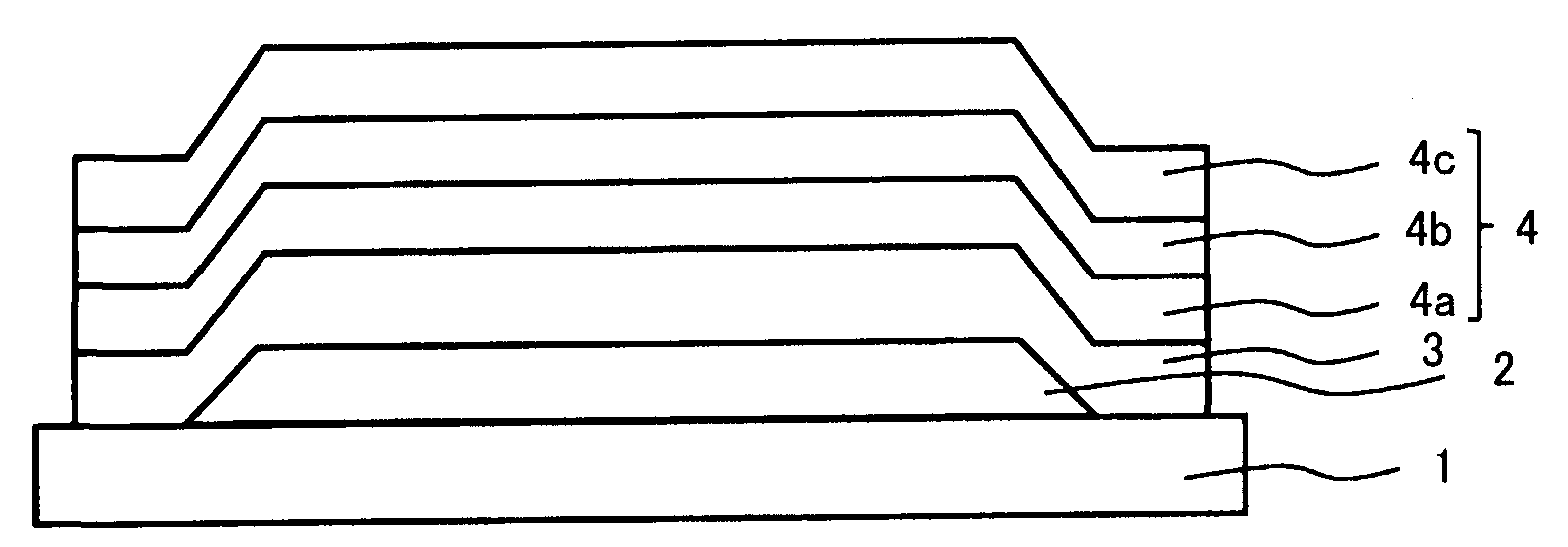
[0072]An organic electroluminescence transparent element having a layer structure as shown in FIG. 1 was prepared by the following method.

(Transparent Substrate 1 and Anode Layer 2)

[0073]First, a glass substrate having formed thereon a patterned transparent electroconductive film (ITO) with a film thickness of 300 nm was subjected to washing treatments in the order of ultrasonic cleaning by pure water and a surfactant, washing with flowing pure water, ultrasonic cleaning by a 1:1 mixed solution of pure water and isopropyl alcohol, and boiling washing by isopropyl alcohol. This substrate was slowly pulled up from the boiling isopropyl alcohol, and dried in isopropyl alcohol vapor, and, finally ultraviolet ozone cleaning was performed.

[0074]This substrate was used as an anode 1 and placed in a vacuum chamber which was evacuated to 1×10⁻⁶ Torr. In this vacuum chamber, each molybdenum boat filled up with a vapor deposition material and a vapor deposition mask for forming a film in a pre...

example 2

[0093]Onto ITO (100 nm) of the cathode layer of the transparent element prepared in Example 1, one where titanium oxide (manufactured by Kanto Chemical Co. Inc.: anatase-type; 0.1-0.3 micrometers in particle size) and fluorinated oil (demnum S-20, manufactured by Daikin Industries, Ltd.) were dewatered, mixed, and defoamed at a low dew point was applied directly, to form an optical diffusion reflection layer having a film thickness of 200 micrometers.

[0094]This was sealed with another glass plate using an UV curing resin, to obtain an organic EL element.

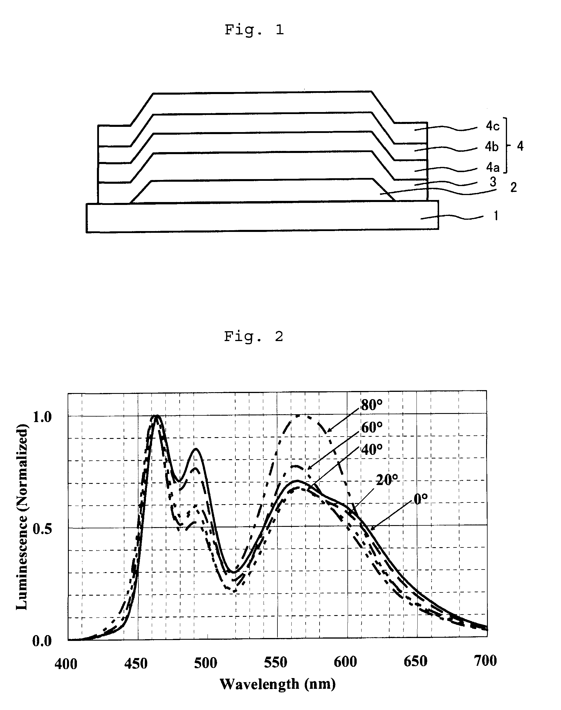
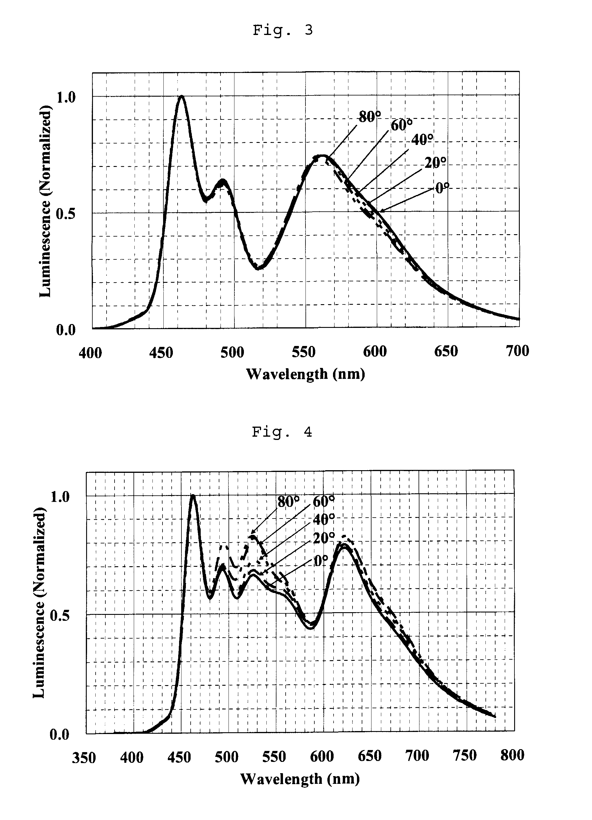
[0095]FIG. 3 shows a graph of the result of evaluating angle dependability of a spectrum of this element.

[0096]As is clear from comparison between FIGS. 2 and 3, in the case where the optical diffusion reflection layer is prepared, it is confirmed that the angle dependability of the spectrum is controlled and it looks the same in color at any angle (in Example 2, FIG. 2),

[0097]Further, external quantum efficiency at a current density...

example 3

[0098]By way of a technique similar to that in Example 1, each electrode layer and a light emitting unit were formed to laminate four light emitting units through a second charge generation layer. Further, the optical diffusion reflection layer was formed by way of a technique similar to that in Example 2, to prepare the organic EL element of a multi-photon structure.

[0099]The above-mentioned second charge generation layer was such that, using Liq as the electron supply substance, DPB:Liq=75:25 were subjected to film formation to have a film thickness of 17 nm, on which an aluminum (Al) film having a film thickness of 0.5 nm was formed. Further, MoO3, as an electron accepting substance, was subjected to film formation independently to have a film thickness of 2 nm and formed between the respective units.

[0100]A layer structure of this element is simplified and shown ITO(300 nm) / MoO3(5 nm) / / first unit (blue) [NS21(15 nm) / EB43:EB52 (30 nm, 98.8:1.2) / BAlq (5 nm)] / / DPB:Liq(17 nm, 75:25)...


PUM

PropertyMeasurementUnit
Work functionaaaaaaaaaa
Permeabilityaaaaaaaaaa
Transparencyaaaaaaaaaa

Abstract

The present invention provides an organic electroluminescence element in which an anode layer 2, a light emitting unit 3, and a cathode layer 4 which each have optical permeability are stacked on a transparent substrate 1, the cathode layer 4 including a first charge generation layer 4a and a cathode 4c. The cathode 4c is formed by way of a facing target sputtering method. Even in the case where a cathode material which has optical permeability is used, the organic electroluminescence element is driven at a low applied voltage, has no angle dependability of an emission spectrum, and has high luminous efficiency.

Description

BACKGROUND OF THE INVENTION[0001]1. Field of the Invention[0002]The present invention relates to an organic electroluminescence (EL) element which can be used suitably for illumination and has optical permeability and to a method of manufacturing the same.[0003]2. Description of the Related Art[0004]Since the organic EL element is a self-luminescence type element which includes an organic compound as a light emitting material and allows luminescence at a high speed, it is suitable for displaying a video image, and it has features that allow an element structure to be simple and a display panel to be thin. Having such outstanding features, the organic EL element is spreading in everyday life as a cellular phone display or a vehicle-mounted display.[0005]Further, in recent years, it has attracted attention as next-generation lighting, taking advantage of the features of thin plane luminescence as described above.[0006]Since one electrode is formed of a reflective electrode made of a m...

Claims


Application Information

Patent Timeline
IPC IPC(8): H01J1/62C23C14/34
CPCH01L51/5092H01L2251/5323H01L51/5221H10K50/171H10K2102/3031H10K50/826H05B33/26H10K50/82
Inventor ODA, ATSUSHIKAWAI, TAKASHITANAKA, JUNICHI
Owner YAMAGATA PROMOTIONAL ORG FOR INDAL TECH
Why Eureka
Try Eureka