Nanoelectronic measurement system for physiologic gases and improved nanosensor for carbon dioxide

a measurement system and physiologic gas technology, applied in the field of sensors, can solve the problems of detection technology use limitations, recall of certain devices, etc., and achieve the effect of inexpensive manufactur

Inactive Publication Date: 2010-03-04
NANOMIX
View PDF52 Cites 30 Cited by
  • Summary
  • Abstract
  • Description
  • Claims
  • Application Information

AI Technical Summary

Benefits of technology

[0014]Furthermore, the described sensors may be conveniently mass-fabricated on tiny substrates, such as a subdivided die of a silicon wafer, lending these sensors to inexpensive manufacture in very small operational packages. The use of silicon wafer technology permits processes and equipment common to the electronics industry to be used. A die comprising the circuitry of one or more sensors may be separated from the wafer. The die may then be pack

Problems solved by technology

Unfortunately there are challenges involved with this approach (see FDA Press Release P04-82 dated Aug. 27, 2004, which is published on the web as http://www.fda.gov/

Method used


Image

  • Nanoelectronic measurement system for physiologic gases and improved nanosensor for carbon dioxide
  • Nanoelectronic measurement system for physiologic gases and improved nanosensor for carbon dioxide
  • Nanoelectronic measurement system for physiologic gases and improved nanosensor for carbon dioxide

Examples


Embodiment Construction

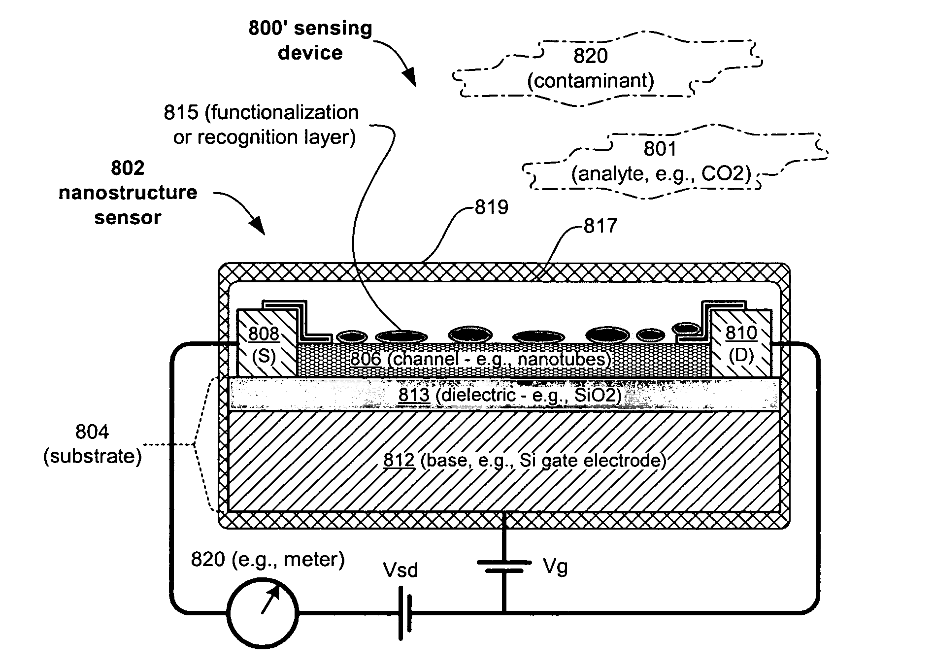
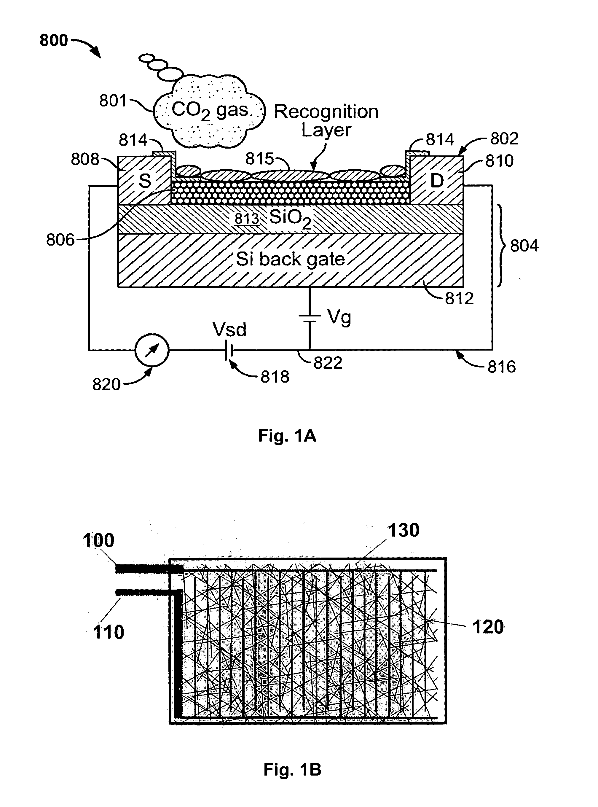
[0034]FIG. 1A schematically illustrates an nanostructure sensor 800, such as is described in U.S. patent application Ser. No. 10 / 940,324, in this example configured as a carbon nanotube field effect transistor or NTFET. FIG. 1A shows an electronic system 800 for detecting carbon dioxide 801, comprising a nanostructure sensing device 802. Device 802 comprises a substrate 804, and a nanostructure 806 disposed over the substrate. The nanostructure may contact the substrate as shown, or in the alternative, may be spaced a distance away from the substrate, with or without a layer of intervening material. In an embodiment of the invention, nanostructure 806 may comprises a carbon nanotube. Any other suitable nanostructure, such as a nanowire, nanofiber, or nanorod, may also be used. In addition, or in the alternative, nanostructure 806 may comprise boron, boron nitride, and carbon boron nitride, silicon, germanium, gallium nitride, zinc oxide, indium phosphide, molybdenum disulphide, silv...


PUM


Abstract

A system for measuring an analyte of interest, particularly carbon dioxide, dissolved in a fluid media of a patient including a nanoelectronic sensor and a measurement instrument in communication with the sensor and configured to receive at least a signal from the sensor indicative of a response of the sensor to at least the analyte of interest.

Description

CROSS-REFERENCE TO RELATED APPLICATIONS[0001]This application is also a continuation-in-part of co-pending U.S. patent application Ser. No. 10 / 656,898 filed Sep. 5, 2003 entitled “Polymer Recognition Layers For Nanostructure Sensor Devices” (published as US 2005-0279,987), which in turn claims priority to Provisional Application No. 60 / 408,547 filed Sep. 5, 2002, which applications are incorporated by reference.[0002]This application is also a continuation-in-part of co-pending U.S. patent application Ser. No. 10 / 773,631 filed Feb. 6, 2004 entitled “Analyte Detection In Liquids With Carbon Nanotube Field Effect Transmission Devices”, which claims priority to U.S. Provisional Patent Application No. 60 / 445,654 filed Feb. 6, 2003, which applications are incorporated by reference.[0003]This application is also a continuation-in-part of co-pending U.S. patent application Ser. No. 10 / 846,072 filed May 14, 2004 entitled “Flexible nanotube transistors” (published as US 2005-0184,641), which...

Claims


Application Information

Patent Timeline
IPC IPC(8): A61B5/05A61N1/36
CPCA61B5/073A61B2562/0285B82Y10/00B82Y15/00H01L51/0545G01N33/5438H01L51/0048H01L51/0052B82Y20/00H10K85/221H10K85/615H10K10/466
Inventor BEN-BARAK, NADAVCHANG, DANIEL M.GABRIEL, JEAN-CHRISTOPHE P.JOSHI, VIKRAMNIEMANN, JOSEPHSTAR, ALEXANDERVALCKE, CHRISTIAN
Owner NANOMIX
Why Eureka
Try Eureka