

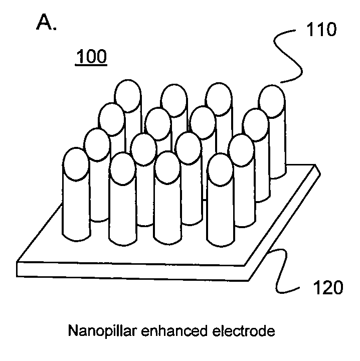
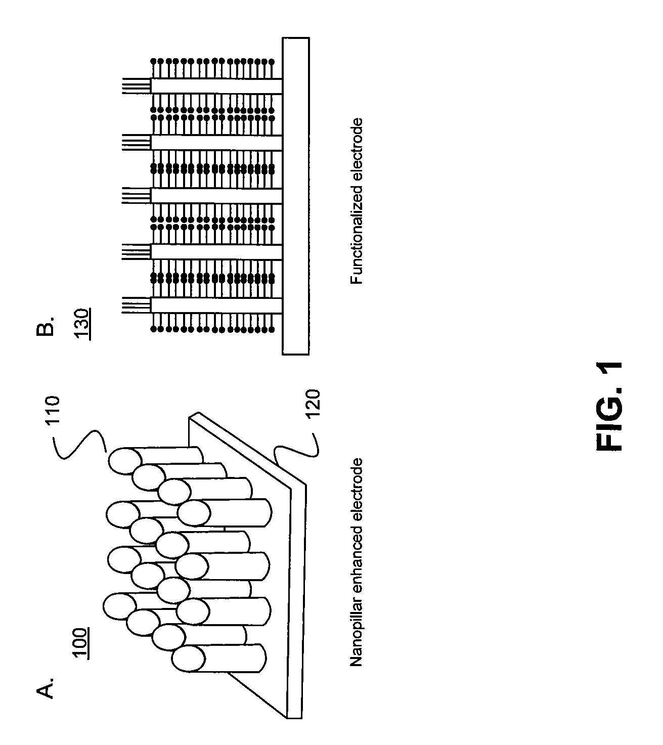
Fabrication of microstructures integrated with nanopillars along with their applications as electrodes in sensors
a nano-pillar and micro-structure technology, applied in the direction of micro-structural devices, vibration measurement in solids, micro-ultrasonic/infrasonic waves, etc., can solve the problems of low sensitivity, poor specificity, prone to fouling, etc., and achieve the effect of increasing detection sensitivity
- Summary
- Abstract
- Description
- Claims
- Application Information
AI Technical Summary
Benefits of technology
Problems solved by technology
Method used
Image

Examples
example 1
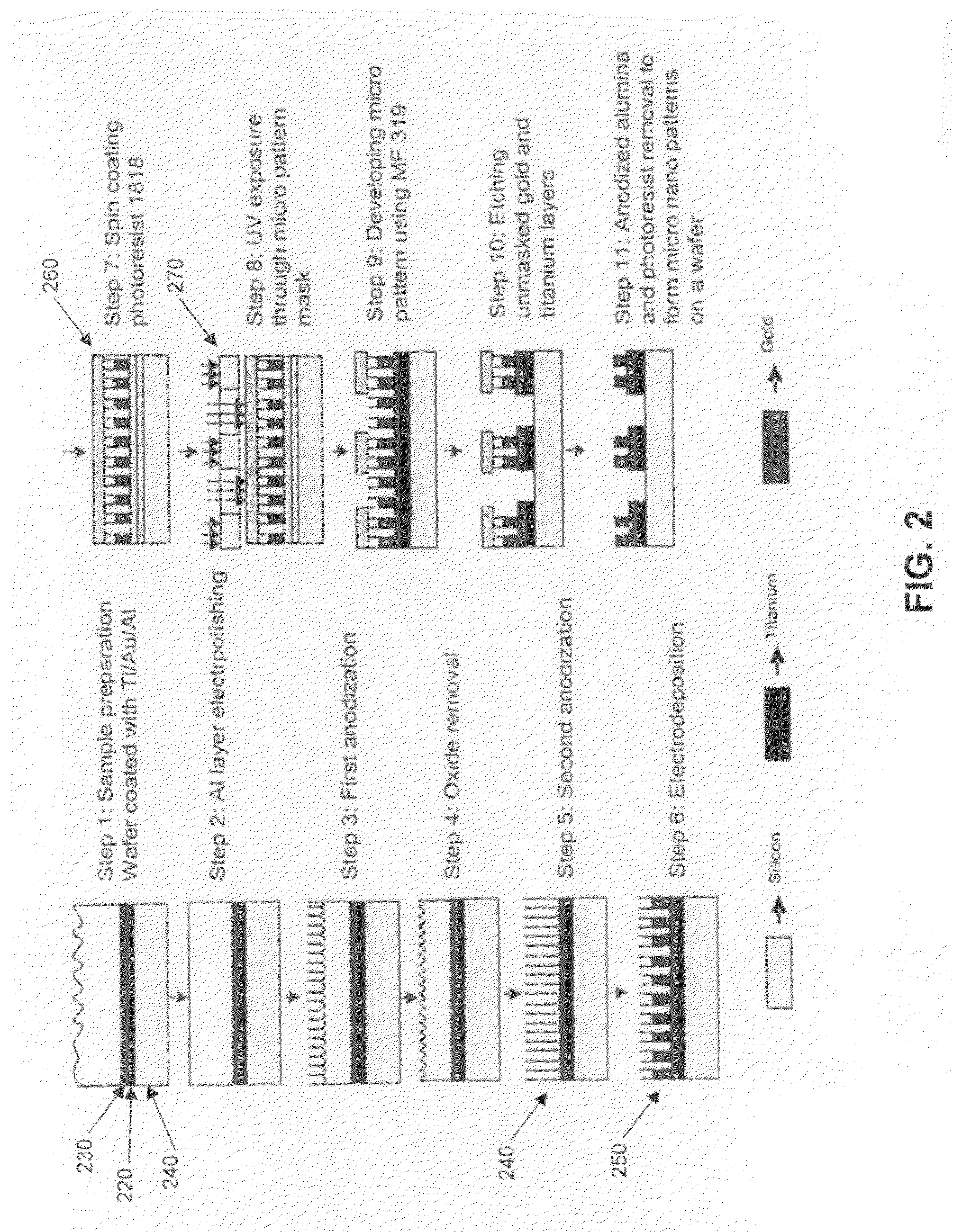
Fabrication Process Used to Integrate Micro and Nanoscale Features Onto a Solid Substrate
[0100]
Step 1:Sample preparation: A silicon wafer 210 is coated with a thin layer of titanium220 (10 nm) followed by a layer of gold 230 (100 nm). Subsequently, a thick layerof aluminum (μm) is coated using an e-beam evaporator.Step 2:Electropolishing: The A1 layer is then electropolished in a 9:1 ethanol to watersolution.Steps 3-5:Anodization: A two-step anodization process is performed at a constant potentialin oxalic acid. The A1 layer is first anodized for a short duration followed by oxidelayer removal using chromic acid solution. Then, second anodization is carriedout all the way to the gold layer, leaving a wafer with the anodized alimunimoxide porous template 240.Step 6:Electrodeposition: Gold nanopillars 250 are formed by electrodeposition into thenanopores in a gold cyanide bath.Steps 7-10:Micro patterning: Photoresist 1818 (positive photoresist) 260 is spin coated onthe sample and then...
example 2
Fabrication of Vertically Aligned Nanopillar Array Structures
[0101]Nanopillar array electrodes (NAEs) with three different pillar heights tested herein were fabricated using a template method [12]. It will be apparent to the skilled artisan that similar results will be obtained with the nanopillar-enhanced electrodes prepared by the process detailed in this invention.
[0102]In fabricating these electrodes, a layer of gold film about 150 nm thick was first sputter-coated onto one side of a porous anodic alumina (PAA) circular disc (d=25 mm; Whatman Inc, Maidstone, England) having an average pore diameter of 150 nM using a SPI sputter coater (Structure probe Inc, West Chester, Pa.). Then, a thicker gold layer was electrodeposited on top of the sputtered gold film to form a strong supporting base in an Orotemp24 gold plating solution (Technic Inc, Cranston, R.I.) with a current density of 5 mA / cm2 for two minutes. This supporting base was masked with Microstop solution (Pyramid plastics...
example 3
Evaluation of the Electrochemical Characteristics of the Nanopillar Array Structures
[0104]The electrochemical characteristics of the developed nanopillar array electrodes (NAE's) were evaluated in a three-electrode electrochemical system with nano-structured electrode used as a working electrode. Cyclic voltammetry (CV) was performed on the NAE's, using a flat gold electrode having the same geometrical area (about 16 mm2) as a control. The flat gold electrode was prepared by depositing a thin film (300 nm) of gold on titanium-coated glass plate using a thermal evaporator (built in-house). CV was performed in 0.5 M Na2SO4 supplemented with 4 mM K4Fe(CN)6 (JT Baker Inc., Phillipsburg, N.J., USA) at various scan rates (50 mV / s, 100 mV / s, 150 mV / s, and 200 mV / s). All runs were conducted in an unstirred solution using high purity deionized water.
[0105]FIG. 8 shows the CVs for three NAE's and a flat electrode. In all these voltammograms, a reduction peak is seen in between 0.70 V and 1.1 ...
PUM
| Property | Measurement | Unit |
|---|---|---|
| thickness | aaaaa | aaaaa |
| thickness | aaaaa | aaaaa |
| thickness | aaaaa | aaaaa |
Abstract
Description
Claims
Application Information