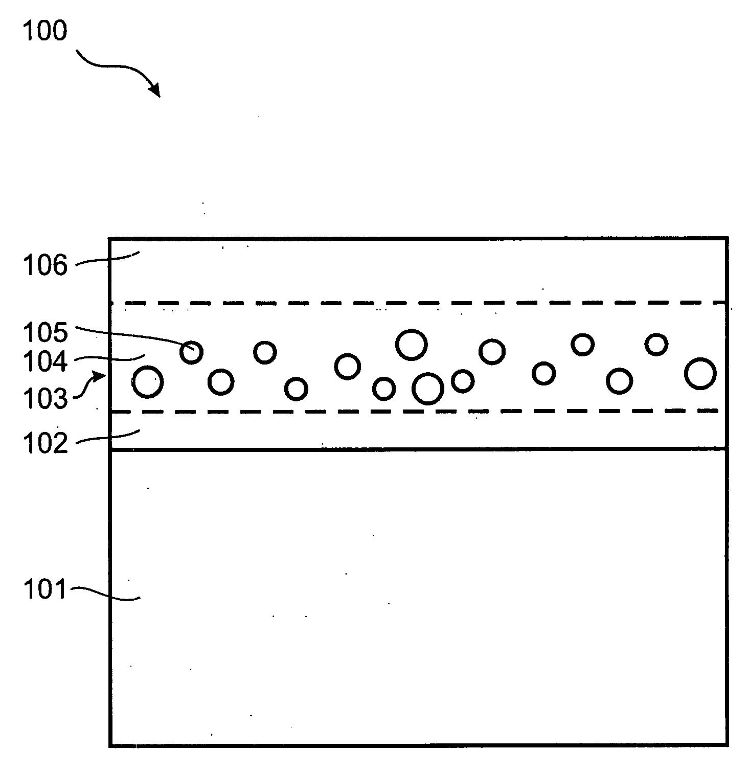
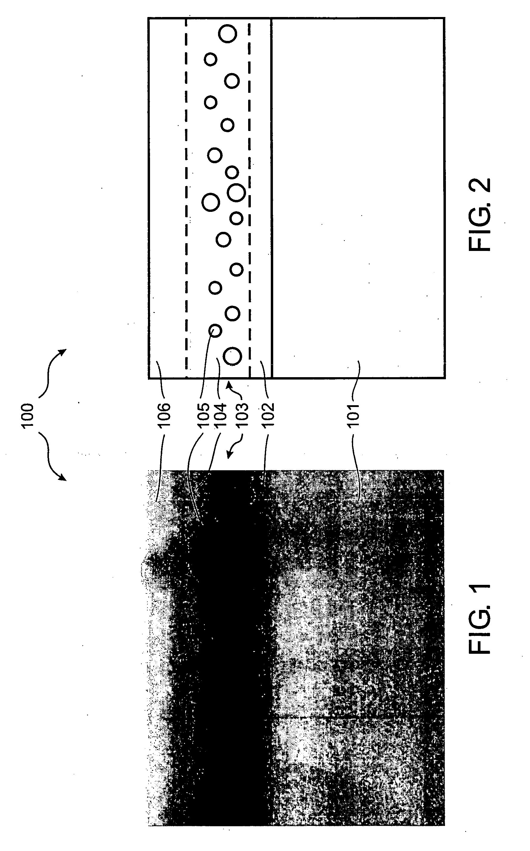
Condensed materials

a technology of oxide films and condensed materials, applied in the direction of fixed capacitors, liquid/solution decomposition chemical coatings, transportation and packaging, etc., can solve the problems of paper not considering ge nanodot formation in thin films, typically requires technical sophistication equipment, and reduces the peak temperature of heat treatment, preventing unwanted electron flow, and shortening the duration of heat treatmen

Inactive Publication Date: 2010-03-18
WESTFALISCHE WILHELMS UNIV MUNSTER
View PDF3 Cites 14 Cited by
  • Summary
  • Abstract
  • Description
  • Claims
  • Application Information

AI Technical Summary

Benefits of technology

[0033]The invention is furthermore directed at such a device that comprises a substrate having a first layer of silicon dioxide on the surface of the substrate and a second layer of silicon dioxide with germanium nanocrystals. The silicon dioxide of the first layer is a dielectric material that prevents unwanted electron flow.
[0034]The first layer of SiO2 develops when the sol-gel layer is consolidated. A thinner first layer can be obtained, if the duration of the heat treatment is shortened, the peak temperature of the heat treatment is decreased, or the oxygen content is reduced during the consolidation phase.

Problems solved by technology

These methods typically need technically sophisticated equipment and are relatively cost-intensive.
However, this paper does not consider Ge nanodot formation in thin films.

Method used


Image

  • Condensed materials
  • Condensed materials

Examples


example 2

[0041]Tetraethoxysilane, germaniumtetraethoxide Ge(OC2H5)4, ethanol, diethoxydimethylsilane (CH3)2Si(OC2H5)2, hydrochloric acid (HCl), and highly purified water were used here as starting materials.

[0042]The diethoxydimethylsilane was diluted with ethanol. Then it was hydrolyzed with water and hydrochloric acid for several hours. The hydrolysis was done under continuous stirring in a closed bottle at 5° C. Afterwards a part of the solution described above and water were added to a solution consisting of tetraethoxysilane, germaniumtetraethoxide and ethanol. This new solution was aged for several hours under the same conditions that were applied for the hydrolysis of diethoxydimethylsilane as described above. Slices of silicon wafers were dip coated with this solution. The thermal treatment was the same as used in example

[0043]1. The presence of hydrolyzed diethoxydimethylsilane lowers the condensation rate of hydrolyzed germaniumtetraethoxide. Without this additive the solutions con...


PUM

PropertyMeasurementUnit
thicknessaaaaaaaaaa
thicknessaaaaaaaaaa
temperaturesaaaaaaaaaa

Abstract

A method for synthesis of germanium nanoparticles in thin SiO2 films comprising: preparing a solution comprising silicon esters, germaniumtetrachloride (GeCl4) or germanium esters, methyl- or higher alcohols, and water; applying the solution to a surface of a substrate; consolidating the solution on the surface of the substrate, thereby obtaining a glass comprising silicon dioxide and germanium dioxide; selectively reducing the germanium dioxide to form germanium nanoparticles.

Description

[0001]The functional properties of materials such as crystalline elemental and compound semi-conductors, ion conducting homogeneous and nanostructured glasses, and silica layers are strongly affected by defects. The understanding about the properties of defects is of fundamental significance for the fabrication of materials with desired features. These defects may be for example group IV nanocrystals that are embedded in SiO2. In the past, one focus has been on silicon nanocrystals in SiO2, but also germanium nanocrystals have been studied. Nanocrystals of this kind show at least two interesting effects. Firstly, it could be shown that nanocrystals can serve as efficient light emitters and are, therefore, interesting for optical applications. Secondly, compatibility with silicon-based electronics can be maintained when using these materials which is of particular interest when the nanoparticles are to be created in a thin film applied to the silicon-based electronic.PRIOR ART[0002]A...

Claims


Application Information

Patent Timeline
Patent Type & Authority Applications(United States)
IPC IPC(8): B32B5/16B05D3/00B05D3/02B05D3/04
CPCB82Y30/00Y10T428/256C01P2004/64C01P2004/90C03C1/008C23C18/02C23C18/1212C23C18/1245C23C18/1266C23C18/1275C23C18/1279C23C18/1291C23C18/1295H01G4/105C01P2004/04B05D3/0453C03C14/006H01L21/02107
Inventor HARTMUT, BRACHTKNEBEL, SEBASTIAN
Owner WESTFALISCHE WILHELMS UNIV MUNSTER
Why Eureka
Try Eureka