Semiconductor device and method for manufacturing same
a semiconductor and device technology, applied in the field of semiconductor devices, can solve the problems of difficult to form a device of a high withstand voltage system, the board area cannot be small, and the whole semiconductor device cannot be made small, and achieve the effect of excellent low power consumption and high speed
- Summary
- Abstract
- Description
- Claims
- Application Information
AI Technical Summary
Benefits of technology
Problems solved by technology
Method used
Image

Examples
first embodiment
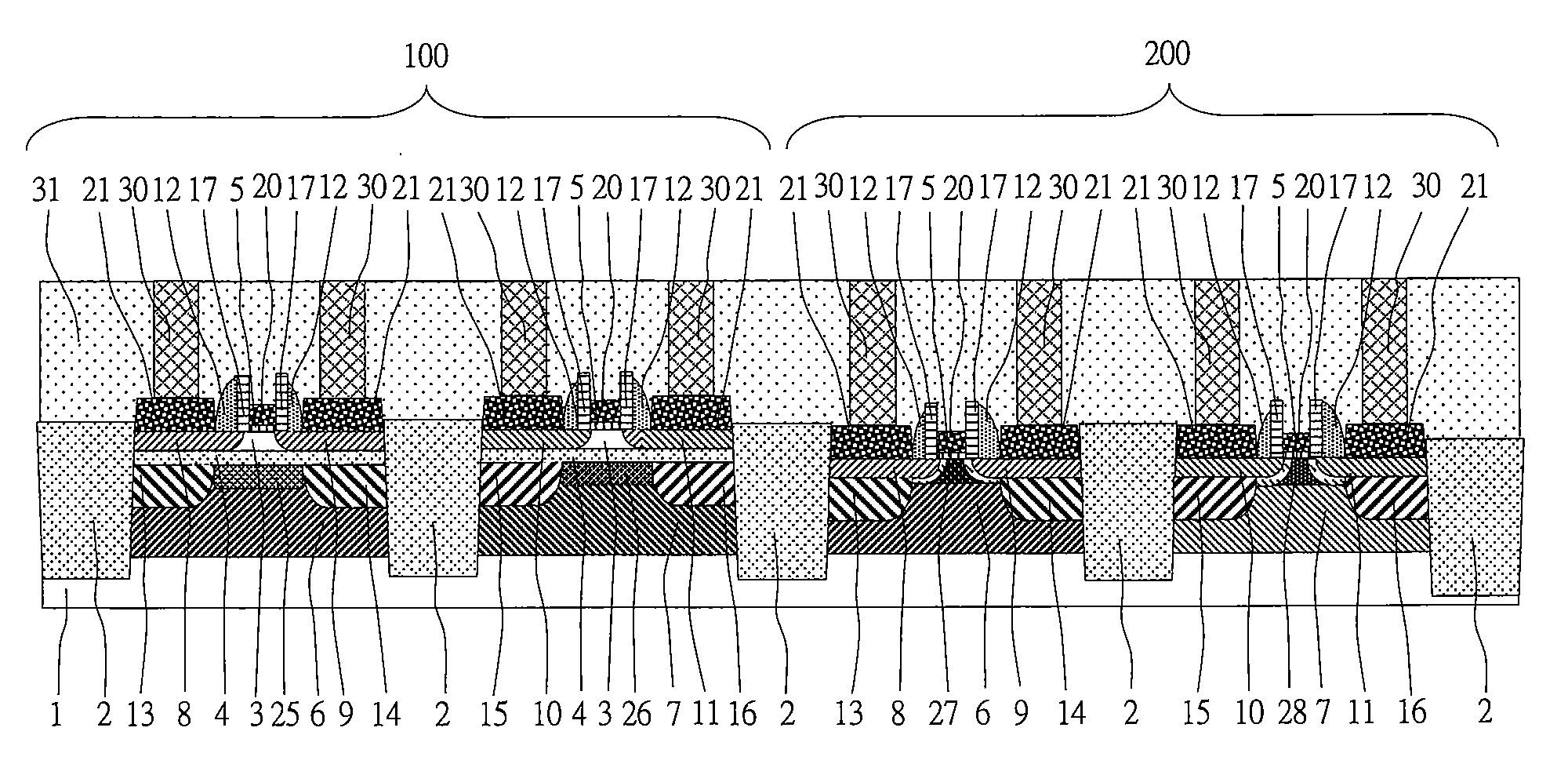
[0057]FIG. 1 is a sectional view showing a completed MISFET according to a first embodiment of the present invention. Manufacturing steps thereof will be described with reference to FIG. 2 and subsequent figures. For convenience of description, description will be made with conductive types of a semiconductor substrate and a semiconductor film being fixed, but the combination of conductive types may be arbitrary, so the conductive type is not limited to the ones described in the present embodiment. A first semiconductor substrate is made by a semiconductor substrate 1 made of single crystal Si having a plane orientation of (100), P conductive type, a resistivity of 10 ohm·cm and a diameter of 20 cm, a main surface thereof has been subjected to mirror polishing, and a thermal oxide film 4 made of silicon having a thickness of 10 nm is formed thereon. Hydrogen ion implantation is performed to the first semiconductor substrate based on a well-known method of manufacturing an ultra-thin...
second embodiment
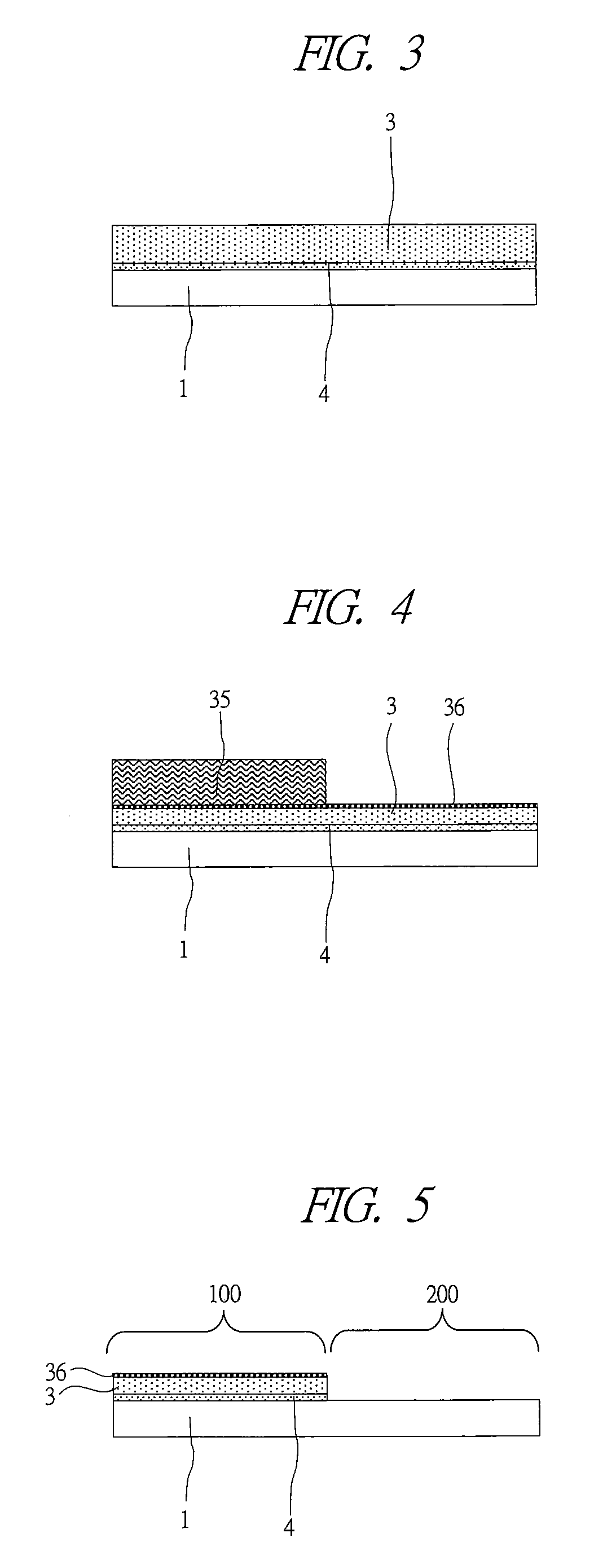
[0075]Next, a semiconductor device according to a second embodiment of the present invention will be described. In the present embodiment, though the semiconductor device is manufactured according to the first embodiment, it has a different layout the second embodiment and has been invented to be capable of forming a bulk-type MISFET more stably. In the present embodiment, the layout at the step of removing the resist mask is different only in the region 200 in FIG. 4 in which the bulk-type MISFET is formed. In the first embodiment, the silicon oxide film 36, the single crystal Si layer 3 and the thin buried insulating film 4 are removed except for the region 200 in which the bulk-type MISFET is formed to expose the supporting substrate surface. On the other hand, in the second embodiment, as shown in the plan view of FIG. 26, a dummy pattern 60 is provided around the region 200 in which the bulk-type MISFET is formed, and the silicon oxide film 36, the single crystal Si layer 3 and...
third embodiment
[0078]FIG. 27 is a sectional view of a semiconductor device showing a third embodiment according to the present invention. In the present embodiment, though the semiconductor device is manufactured basically in a similar manner as the abovedescribed embodiments, in the third embodiment, prior to formations of the ultra-shallow N-conductive type high-concentration source diffusion layer 8 and the ultra-shallow N-conductive type high-concentration drain diffusion layer 9, and the ultra-shallow P-conductive type high-concentration source diffusion layer 10 and the ultra-shallow P-conductive type high-concentration drain diffusion layer 11, formation of an offset spacer 17 are performed on sidewalls of the gate electrode. The offset spacer 17 is formed on the sidewalls of the gate electrode by depositing, for example, a silicon oxide film, a silicon nitride, a titanium oxide film, or the like by about 10 nm by CVD method and etching back the insulating film. The ultra-shallow high-conce...
PUM
 Abstract
Description
Claims
Application Information
 - Generate Ideas
- Intellectual Property
- Life Sciences
- Materials
- Tech Scout
- Unparalleled Data Quality
- Higher Quality Content
- 60% Fewer Hallucinations
Browse by: Latest US Patents, China's latest patents, Technical Efficacy Thesaurus, Application Domain, Technology Topic, Popular Technical Reports.
© 2025 PatSnap. All rights reserved.Legal|Privacy policy|Modern Slavery Act Transparency Statement|Sitemap|About US| Contact US: help@patsnap.com