Advanced platform for processing crystalline silicon solar cells

a technology of solar cells and crystalline silicon, applied in the field of advanced platform for processing crystalline silicon solar cells, can solve the problems of increasing the cost of producing and supporting all of the processing components in the production line, and the serious challenges of silicon wafer production development for photovoltaics

Inactive Publication Date: 2010-04-08
APPLIED MATERIALS INC
View PDF16 Cites 91 Cited by
  • Summary
  • Abstract
  • Description
  • Claims
  • Application Information

AI Technical Summary

Problems solved by technology

The high market growth rate in combination with the need to substantially reduce solar electricity costs has resulted in a number of serious challenges for silicon wafer production development for photovoltaics.
However, the cost associated with producing and supporting all of the processing components in a solar cell production line continues to escalate dramatically.

Method used


Image

  • Advanced platform for processing crystalline silicon solar cells
  • Advanced platform for processing crystalline silicon solar cells
  • Advanced platform for processing crystalline silicon solar cells

Examples


Embodiment Construction

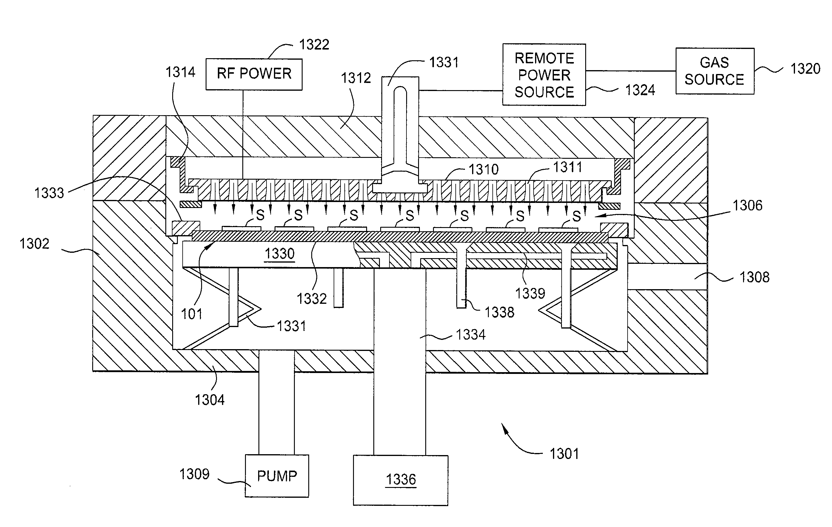
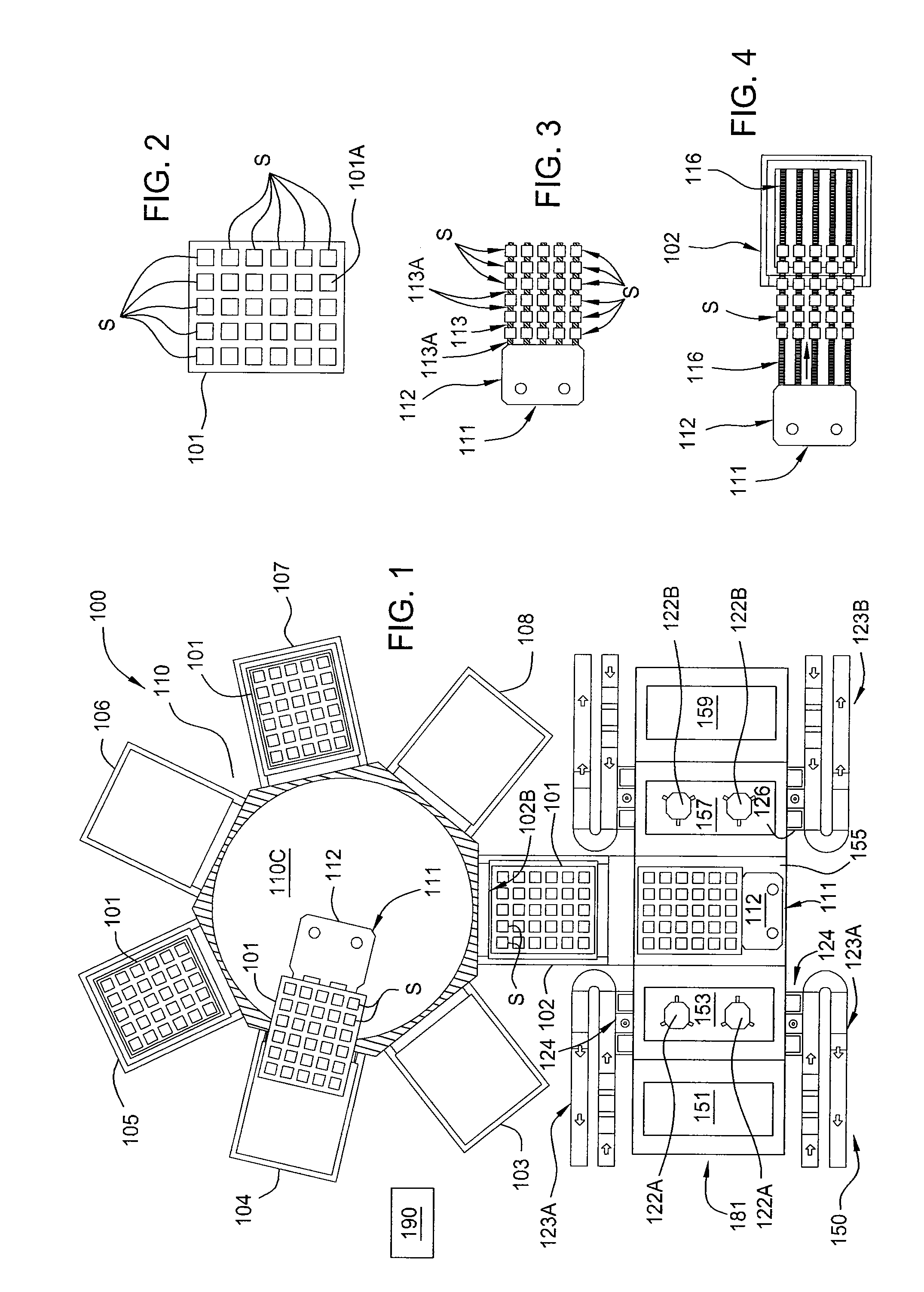
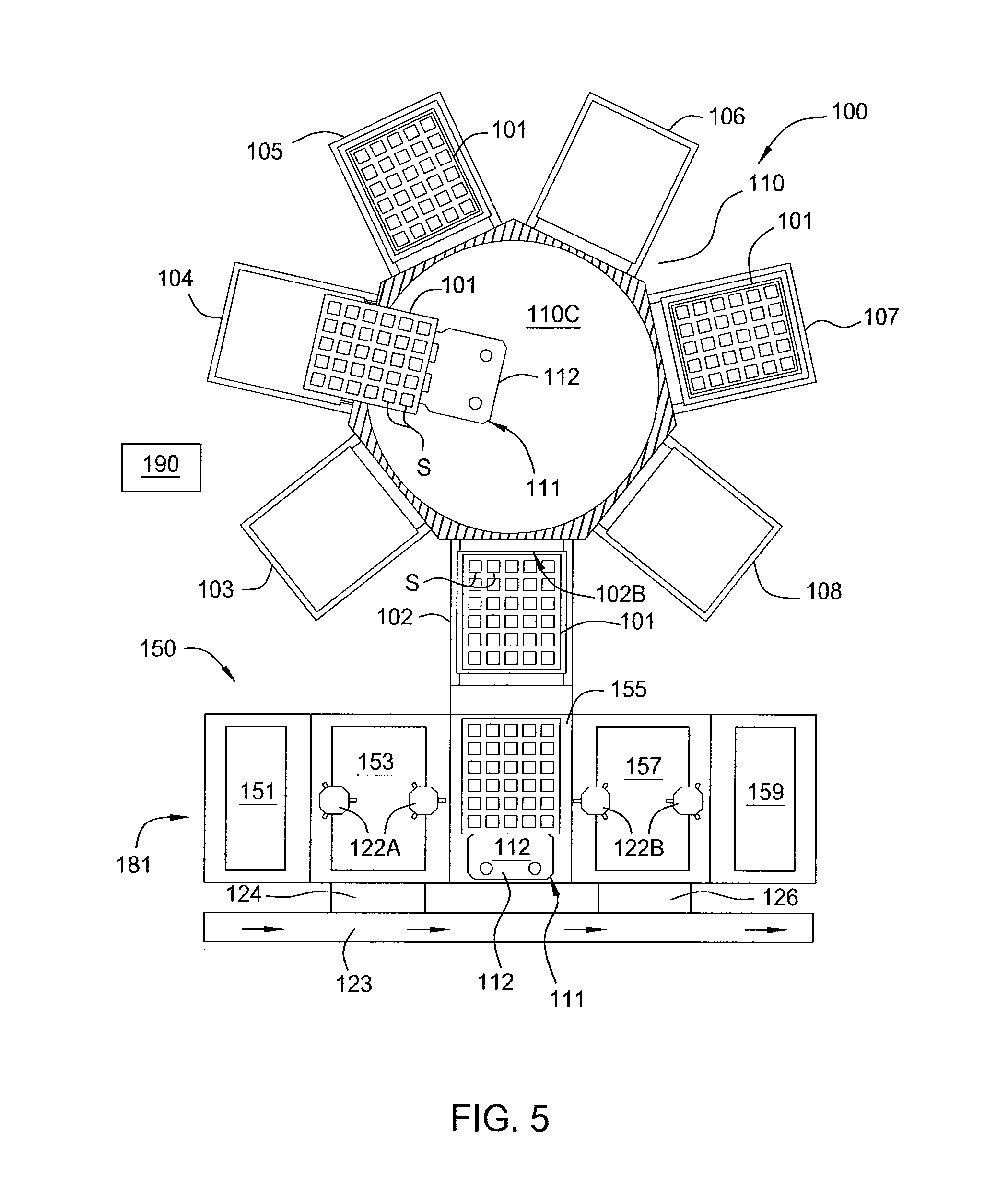
[0027]The present invention generally provides a batch substrate processing system, or cluster tool, for in-situ processing of a film stack used to form regions of a solar cell device. In one configuration, a film stack formed on each of the substrates in the batch contains one or more passivating or dielectric layers and one or more metal layers that are deposited and further processed within various processing chambers contained in the processing system. The processing chambers may be, for example, physical vapor deposition (PVD) or sputtering chambers, plasma enhanced chemical vapor deposition (PECVD) chambers, low pressure chemical vapor deposition (LPCVD) chambers, hot wire chemical vapor deposition (HWCVD) chambers, ion implant / doping chambers, plasma nitridation chambers, atomic layer deposition (ALD) chambers, plasma or vapor chemical etching chambers, laser anneal chambers, rapid thermal oxidation (RTO) chambers, rapid thermal nitridation (RTN) chambers, rapid thermal annea...


PUM


Abstract

The present invention generally provides a batch substrate processing system, or cluster tool, for in-situ processing of a film stack used to form regions of a solar cell device. In one configuration, the film stack formed on each of the substrates in the batch contains one or more silicon-containing layers and one or more metal layers that are deposited and further processed within the various chambers contained in the substrate processing system. The processing chambers may be, for example, physical vapor deposition (PVD) or sputtering chambers, plasma enhanced chemical vapor deposition (PECVD) chambers, low pressure chemical vapor deposition (LPCVD) chambers, hot wire chemical vapor deposition (HWCVD) chambers, plasma nitridation (DPN) chambers, ion implant / doping chambers, atomic layer deposition (ALD) chambers, plasma etching chambers, annealing chambers, rapid thermal oxidation (RTO) chambers, rapid thermal annealing (RTA) chambers, substrate reorientation chambers, laser annealing chambers, and / or plasma cleaning stations. In one embodiment, a batch of solar cell substrates is simultaneously transferred in a vacuum or inert environment to prevent contamination from affecting the solar cell formation process.

Description

CROSS-REFERENCE TO RELATED APPLICATIONS[0001]This application claims benefit of U.S. Provisional Patent Application Ser. No. 61 / 103,498 [Attorney Docket #: APPM 13855L], filed Oct. 7, 2008, which is herein incorporated by reference in its entirety.BACKGROUND OF THE INVENTION[0002]1. Field of the Invention[0003]Embodiments of the invention generally relate to an apparatus and method for forming a solar cell device. The invention is particularly useful for fabrication of crystalline silicon solar cells processed in batches arranged in planar arrays.[0004]2. Description of the Related Art[0005]Photovoltaic (PV) or solar cells are devices which convert sunlight into direct current (DC) electrical power. A typical PV cell includes a p-type silicon wafer, or substrate, typically less than about 0.3 mm thick, with a thin layer of an n-type silicon material disposed on top of the p-type substrate. The generated voltage, or photo-voltage, and generated current by the PV cell are dependent on...

Claims


Application Information

Patent Timeline
Patent Type & Authority Applications(United States)
IPC IPC(8): H01L31/18H01L21/677
CPCH01L21/67069H01L21/67167H01L21/67201Y02E10/50H01L21/67236H01L31/1876H01L21/67213Y02P70/50
Inventor PORTHOUSE, KEITH BRIANBORDEN, PETER G.HOLTAM, TRISTAN R.ZHOU, LISONGLATCHFORD, IAN SCOTTAQUI, DEREKSHAH, VINAY K.
Owner APPLIED MATERIALS INC
Why Eureka
Try Eureka