In addition to their often high cost, all these techniques present numerous problems that render them incompatible with the
microfabrication processes of electronic circuits and integrated circuits on
silicon wafers, save at the expense of substantial alterations of the treated supports and the electronic circuits therein included.
In addition, from the structural point of view, the porous materials grown or deposited with the existing techniques present numerous defects such as partial or
total occlusion of the pores, non-reproducibility, non-uniformity of the layers and poor process flexibility (in terms of
insertion in the current production cycles of electronic devices including them).
For example, spray deposition implies a substantial modification of the manufacturing cycle of integrated electronic circuits due to the introduction of a deposition
system that is infrequent in these manufacturing processes and to the problems related to polluting
volatile solvents, the disposal of which, in this type of deposition, requires particular control operations.
Another problem of this technique consists in the need to heat the substrate to high temperatures during deposition and this may, in some cases, increase the harmfulness of the solvents used, and, in other cases, damage the electronic circuits already integrated on the
semiconductor support.
Direct deposition of solutions is used more frequently, but requires excessive operator intervention and fails to guarantee the necessary reproducibility, whereas growth of the deposition product directly on the silicon substrate, used in some cases as the base of the
autoclave employed for the crystallisation process, is time-consuming, expensive and inapplicable in an industrial manufacturing process of integrated electronic circuits, but is useful only for research purposes in the laboratory.
Thus, in-situ crystallisation and other processes of a hydrothermal nature used for the production of devices on silicon wafers present limitations in terms of their poor compatibility with the manufacturing processes of integrated electronic circuits and therefore also of integrated sensors.
The
sputtering technique, though compatible with
integrated circuit technology, is expensive and introduces additional steps in the
processing of electronic microcircuits which require operator intervention on high-vacuum machines with a resulting increase in production costs, without considering that this technique may damage the integrated circuits to which it is applied.
On account of its complexity and the high temperatures required for
calcination, this process is not compatible with the production techniques of integrated electronic circuits, which do not support maximum working temperatures over 70-80° C. for uses in the commercial field or even above 125° C. for uses in the military field (Horowitz P. and Hill W.
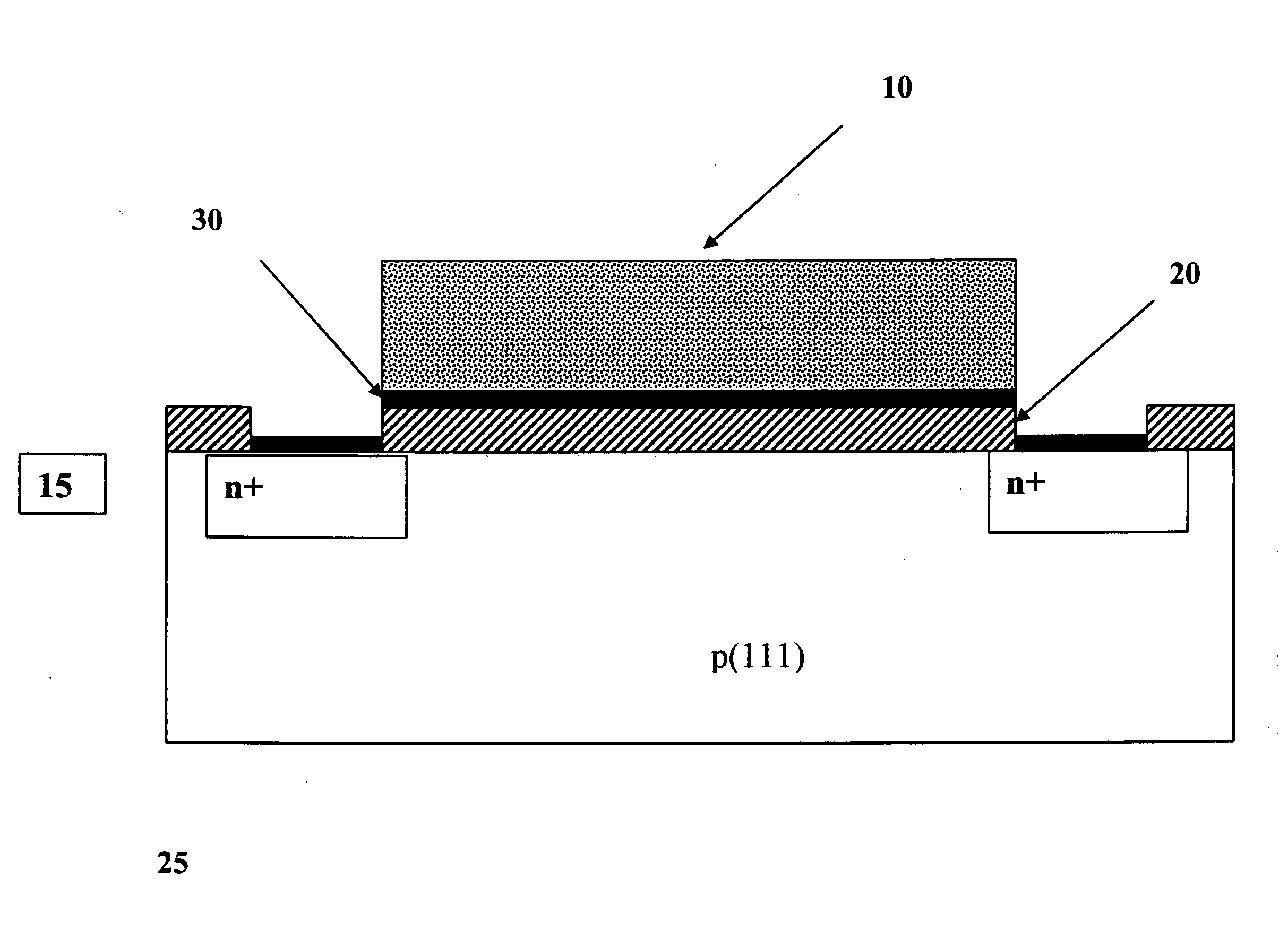
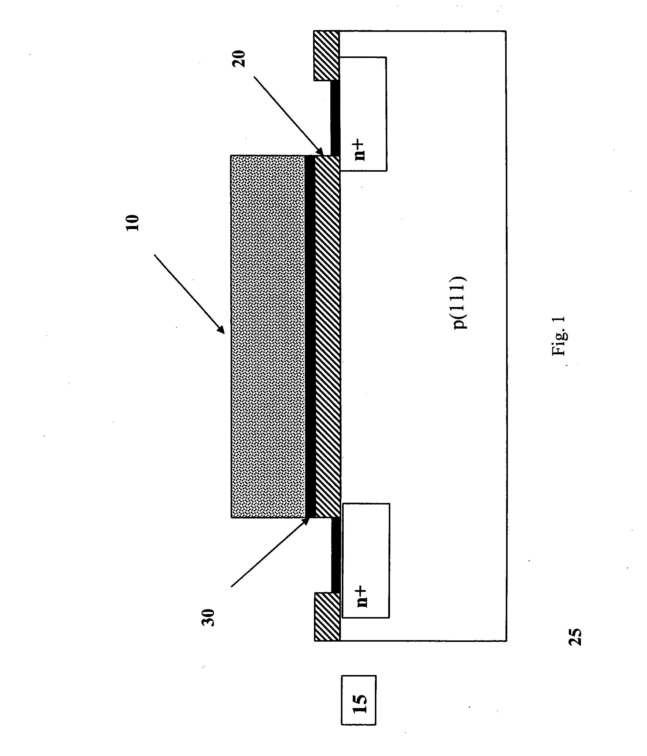
None of the existing techniques, then, makes it possible to obtain uniform layers of zeolites at low cost, with a procedure that is simple, rapid, reproducible in terms of end products and compatible with current production technologies of integrated
microelectronic circuits on silicon wafers, or other
semiconductor materials, such as, for example,
gallium arsenide or
germanium, or on non-conductor supports and supports with planar geometry or variously complex geometries or geometries other than planar, e.g. cylindrical, for the production of sensors or integrated electronic devices.

