Method for manufacturing a semiconductor integrated circuit device circuit device

a semiconductor integrated circuit and circuit device technology, applied in the direction of semiconductor devices, basic electric elements, electrical appliances, etc., can solve the problems of increasing the leakage current between the source/drain the metal silicide layer is partially abnormally grown, and the unfavorable high-speed operation of the field-effect transistor. , to achieve the effect of increasing the scale of the integration of the semiconductor integrated circuit device, reducing and increasing the resistance of the ga

Active Publication Date: 2010-05-27
RENESAS ELECTRONICS CORP
View PDF6 Cites 131 Cited by
  • Summary
  • Abstract
  • Description
  • Claims
  • Application Information

AI Technical Summary

Benefits of technology

[0031]With an increase in scale of integration of a semiconductor integrated circuit device, a field-effect transistor (MISFET: Metal Insulator Semiconductor Field Effect Transistor) is miniaturized according to the scaling rule. However, the resistance of a gate or a source/a drain increases. Thus, even miniaturization of the field-effect transistor unfavorably cannot provide high-speed oper

Problems solved by technology

Thus, even miniaturization of the field-effect transistor unfavorably cannot provide high-speed operation.
In various heating steps (steps involving heating of a semiconductor substrate, such as various insulation film and conductive film deposition steps) after deposition of the silicon nitride film, the metal silicide layer partially abnormally grows due to oxygen in the natural oxide film occurring on the metal silicide layer surface.
Further, when the metal silicide layer has abnormally grown at the ch

Method used


Image

  • Method for manufacturing a semiconductor integrated circuit device
circuit device
  • Method for manufacturing a semiconductor integrated circuit device
circuit device
  • Method for manufacturing a semiconductor integrated circuit device
circuit device

Examples


Embodiment Construction

Summary of Embodiments

[0062]First, summaries will be described on representative embodiments of the invention disclosed in the present application.

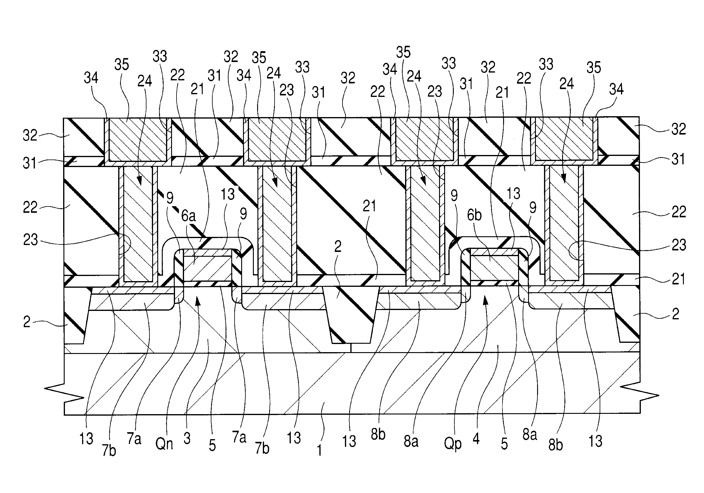
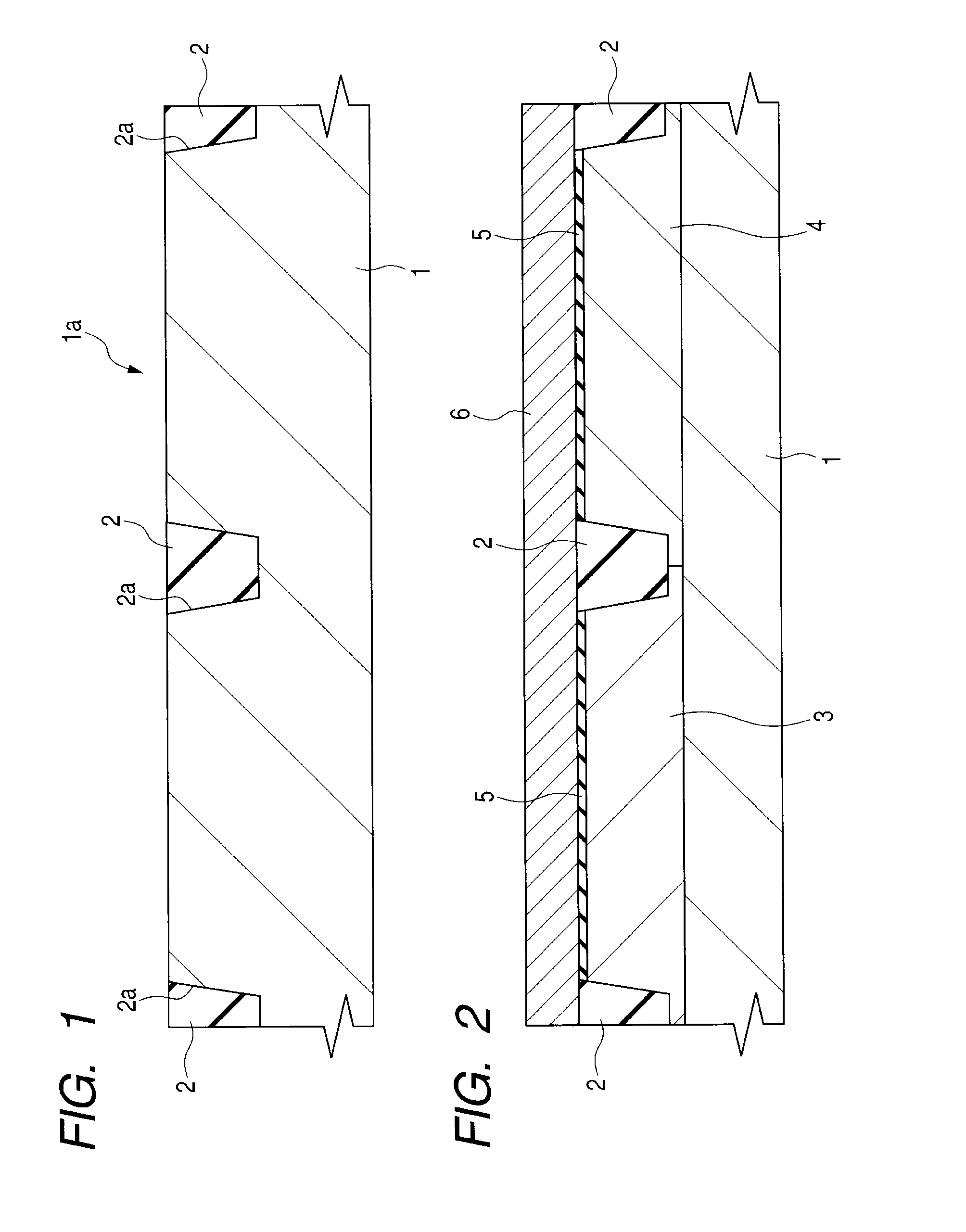
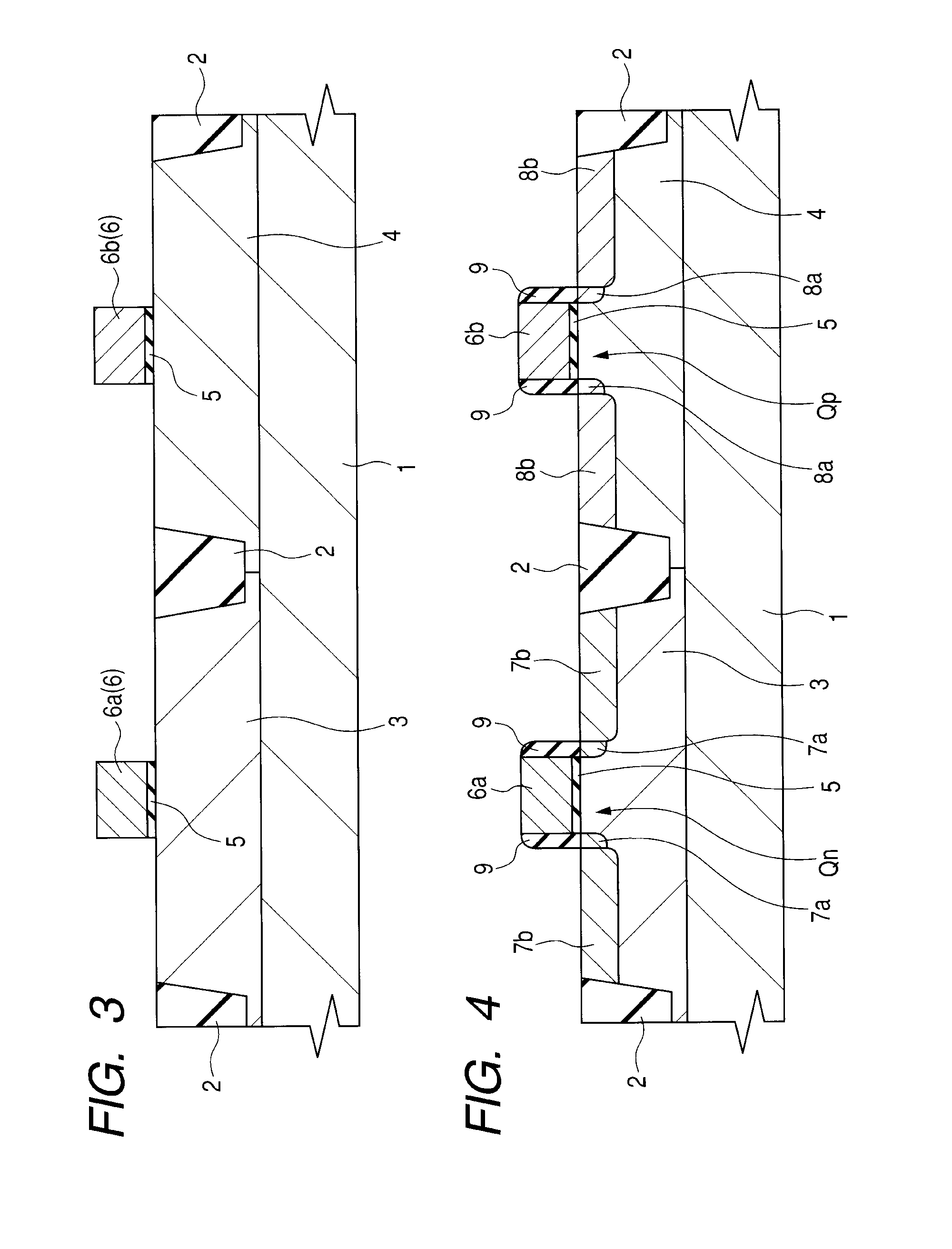
[0063]1. A method for manufacturing a semiconductor integrated circuit device, which includes the steps of: (a) forming a MISFET in a region in the vicinity of a first main surface of a semiconductor wafer, the MISFET having (x1) source / drain regions disposed in a surface region of the first main surface, (x2) a gate insulation film disposed over the first main surface, (x3) a gate electrode including silicon as a main component and disposed over the gate insulation film, and (x4) a silicide film disposed over the source / drain regions; (b) after the step (a), setting the semiconductor wafer over a first lower electrode in a first gas phase treatment chamber with the first main surface facing upward; (c) after the step (b), while the semiconductor wafer being set over the first lower electrode grounded with the first main surface facing up...


PUM


Abstract

When a natural oxide film is left at the interface between a metal silicide layer and a silicon nitride film, in various heating steps (steps involving heating of a semiconductor substrate, such as various insulation film and conductive film deposition steps) after deposition of the silicon nitride film, the metal silicide layer partially abnormally grows due to oxygen of the natural oxide film occurring on the metal silicide layer surface. A substantially non-bias (including low bias) plasma treatment is performed in a gas atmosphere containing an inert gas as a main component on the top surface of a metal silicide film of nickel silicide or the like over source/drain of a field-effect transistor forming an integrated circuit. Then, a silicon nitride film serving as an etching stop film of a contact process is deposited. As a result, without causing undesirable cutting of the metal silicide film, the natural oxide film over the top surface of the metal silicide film can be removed.

Description

CROSS-REFERENCE TO RELATED APPLICATIONS[0001]The disclosure of Japanese Patent Application No. 2008-300439 filed on Nov. 26, 2008 including the specification, drawings and abstract is incorporated herein by reference in its entirety.BACKGROUND OF THE INVENTION[0002]The present invention relates to a technology effectively applicable to a metal silicide-related technology in a method for manufacturing a semiconductor integrated circuit device (or a semiconductor device).[0003]Japanese Unexamined Patent Publication No. 2003-86569 (Patent Document 1) or U.S. Pat. No. 7,122,477 (Patent Document 2) discloses a technology regarding a plasma treatment method for removing a natural oxide film on a CoSi2 film surface.[0004]Japanese Unexamined Patent Publication No. Hei 10 (1998)-112446 (Patent Document 3) discloses a technology in which a TiN layer is formed after removal of a TiOx layer over a Ti silicide layer.[0005]Japanese Unexamined Patent Publication No. 2001-284284 (Patent Document 4)...

Claims


Application Information

Patent Timeline
IPC IPC(8): H01L21/336
CPCH01L21/67167H01L21/823807H01L29/7843H01L21/823835H01L21/823814
Inventor FUTASE, TAKUYAMURATA, SHUHEIHAYASHI, TAKESHI
Owner RENESAS ELECTRONICS CORP
Why Eureka
Try Eureka