Organic electroluminescence device and luminescence apparatus

a luminescence apparatus and electroluminescence technology, applied in the direction of electrical apparatus, thermoelectric device junction materials, semiconductor devices, etc., can solve the problem of excessive energy emitted

Active Publication Date: 2010-06-10
UDC IRELAND
View PDF11 Cites 43 Cited by
  • Summary
  • Abstract
  • Description
  • Claims
  • Application Information

AI Technical Summary

Benefits of technology

On the other hand, in order to sufficiently achieve the effect of the invention, by suppressing the energy transfer of excitons among the phosphorescent materials included in the luminescent layer and obtaining the color of emitted light based on each of the phosphorescent materials, the difference in the maximum value and the minimum value of T1 of the two or more kinds of phosphorescent material included in the luminescent layer is preferably 0.2 eV or more, more preferably 0.5 eV or more, further preferably 0.7 eV or more.
, by suppressing the energy transfer of excitons among the phosphorescent materials included in the luminescent layer and obtaining the color of emitted light based on each of the phosphorescent materials, the difference in the maximum value and the minimum value of T1 of the two or more kinds of phosphorescent material included in the luminescent layer is preferably 0.2 eV or more, more preferably 0.5 eV or more, further preferably 0.7 eV or more.
In the following, each of the materials that form luminescent layer 30 is described in detail.
Exemplary phosphorescent materials used in the present invention include a complex including a transition metal atom or a lanthanoid atom.
Preferable examples of the transition metal atom include, but not particularly limited to, ruthenium, rhodium, palladium, tungsten, rhenium, osmium, iridium and platinum. Among these, rhenium, iridium and platinum are more preferred.
Examples of the lanthanoid atom include lanthanum, cerium, praseodymium, neodymium, samarium, europium, gadolinium, terbium, dysprosium, holmium, erbium, thulium, ytterbium, and lutetium. Among these, neodymium, europium and gadolinium are preferred.

Problems solved by technology

When a voltage is applied between the electrodes, excitons are generated in the luminescent layer positioned between the electrodes, as a result of re-combination of holes and electrons, and excessive energy is emitted as light when the excitons return from the excited state to the ground state.

Method used


Image

  • Organic electroluminescence device and luminescence apparatus
  • Organic electroluminescence device and luminescence apparatus
  • Organic electroluminescence device and luminescence apparatus

Examples


first exemplary embodiment

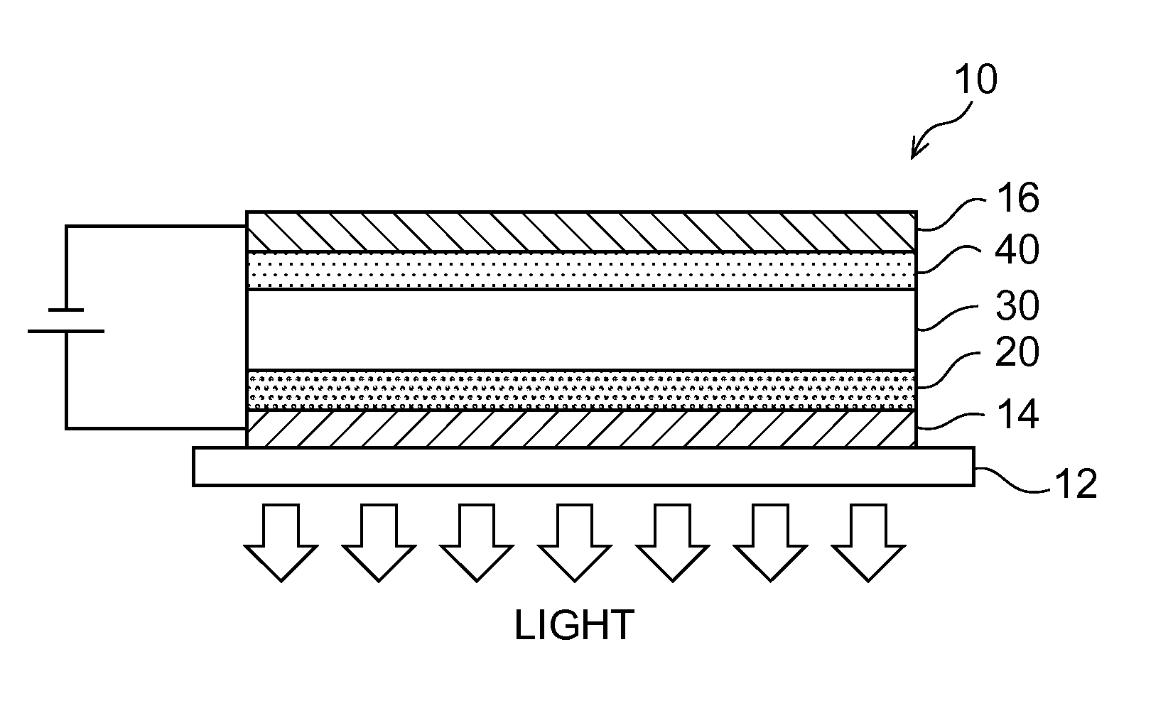
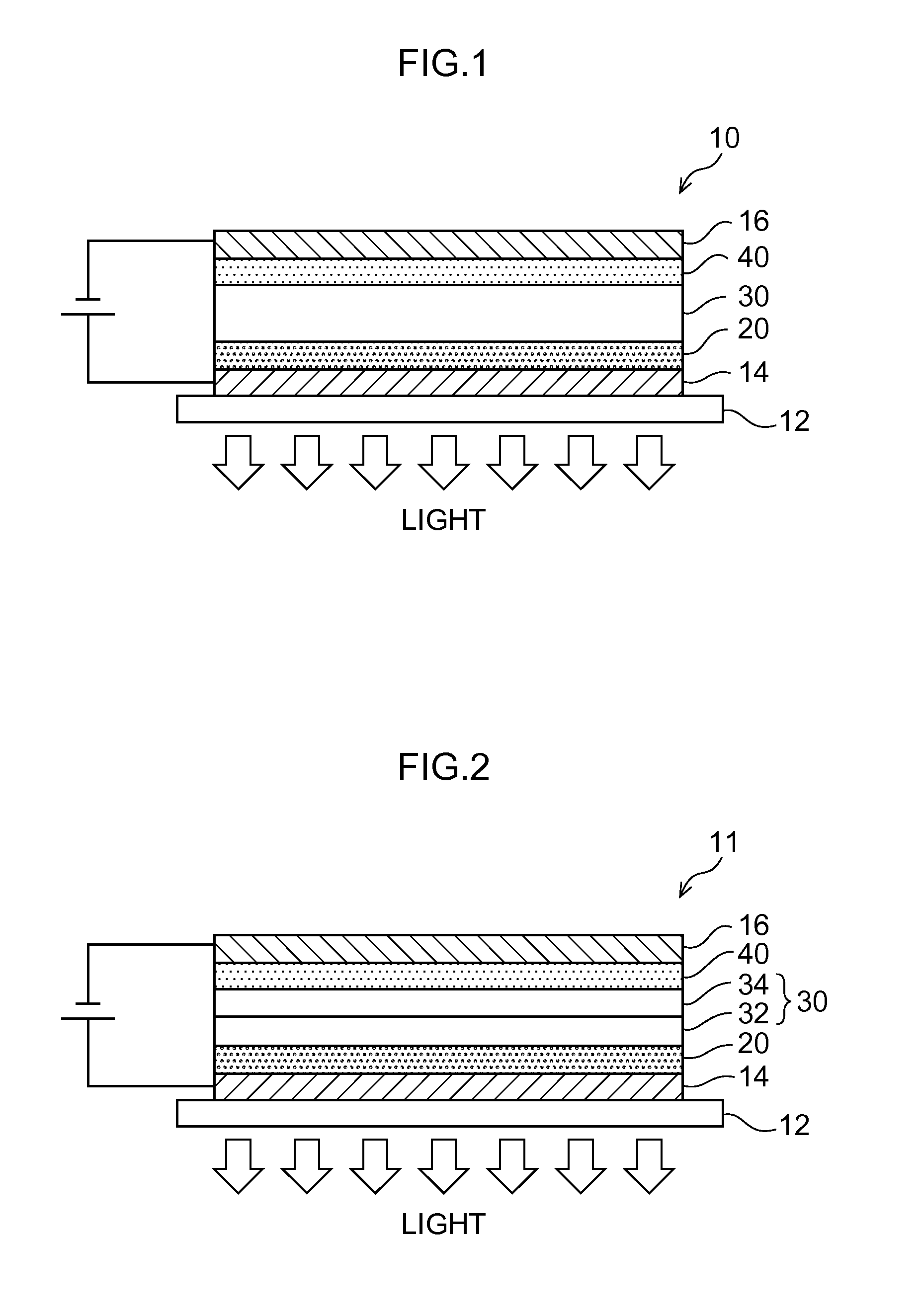
FIG. 1 schematically shows an exemplary structure of the organic EL device according to the invention (first exemplary embodiment). Organic EL device according to the present exemplary embodiment 10 is formed on support substrate 12, and includes a pair of electrodes 14 and 16 located to face each other and an organic layer (including hole-transporting layer 20, luminescent layer 30 and electron-transporting layer 40) located between electrodes 14 and 16.

In the following explanations, an anode is formed on support substrate 12 as lower electrode 14, but it is also possible to form a cathode on support substrate 12 as lower electrode 14.

—Luminescent Layer—

Luminescent layer 30 has a function of receiving holes from the anode, the hole injection-layer or the hole-transporting layer, while receiving electrons from the cathode, the electron-injection layer or the electron-transporting layer, and providing a place at which the holes and the electrons are re-combined to emit light.

The orga...

second exemplary embodiment

FIG. 2 shows a schematic view of a further exemplary embodiment of the organic EL device according to the invention (second exemplary embodiment). Organic EL device 11 according to this exemplary embodiment includes, as luminescent layer 30, two luminescent layers positioned adjacent to each other (first luminescent layers 32 and second luminescent layer 34). In this case, at least one of the luminescent layers includes two or more kinds of phosphorescent material having different T1 values, a binder material, and a charge-transporting material, and has a luminescence spectrum having a peak length based on each of the two or more phosphorescent materials.

The phosphorescent materials included in respective luminescent layers 32 and 34 may be selected according to usage or the like. For example, in order to emit white light by mixing the colors of RGB, it is preferred that the first luminescent layer includes a blue phosphorescent material having a luminescence peak in a range of from...

example 1

An organic EL device having the above standard structure was prepared. The structure of the luminescent layer was as follows.

Luminescent layer: H-4+25%A-1+15%B-1+5%G-1+1%R-1 (30 nm)

The organic EL device was allowed to emit light upon application of a direct voltage using a source measure unit (product type: 2400, manufactured by Toyo Corporation), and the luminance thereof was measured using a measurement device (product type: BM-8, manufactured by Topcon Corporation). The luminescence spectrum and the wavelength were measured using a spectrum analyzer (product type: PMA-11, manufactured by Hamamatsu Photonics K.K.)

The chromaticity based on the CIE 1931 chromaticity coordinate was (x, y)=(0.31, 0.36). The luminescence intensity ratio at luminescence peaks of 456 nm, 503 nm and 620 nm was 0.72:1:0.79, and the color of emitted light in total was white.


PUM

PropertyMeasurementUnit
triplet energy levelaaaaaaaaaa
luminescence peak wavelengthaaaaaaaaaa
ionization potentialaaaaaaaaaa

Abstract

The invention provides an organic EL device including a pair of electrodes and at least one luminescent layer between the pair of electrodes, the at least one luminescent layer including at least two phosphorescent materials, an electrically inert material, and a charge-transporting material, the at least two phosphorescent materials being selected from a blue phosphorescent material having a luminescence peak in a range of from 420 nm to less than 500 nm, a green phosphorescent material having a luminescence peak in a range of from 500 nm to less than 570 nm, or a red phosphorescent material having a luminescence peak in a range of from 570 nm to 650 nm. The invention also provides a luminescence apparatus including the above organic EL device.

Description

CROSS-REFERENCE TO RELATED APPLICATIONThis application claims priority under 35 USC 119 from Japanese Patent Application No. 2008-314812 filed Dec. 10, 2008, the disclosure of which is incorporated by reference herein.TECHNICAL FIELDThe present invention relates to an organic electroluminescence device and a luminescence apparatus.BACKGROUND ARTApparatuses employing an organic electroluminescence device (organic EL device) have been developed in recent years. For example, these apparatuses are formed by providing, on a substrate of glass or the like, an anode, an organic layer (such as a hole-transporting layer, a luminescent layer and an electron-transporting layer), a cathode, and the like, and connecting the same with an external wiring via wirings (terminals) of the two electrodes. When a voltage is applied between the electrodes, excitons are generated in the luminescent layer positioned between the electrodes, as a result of re-combination of holes and electrons, and excessive...

Claims


Application Information

Patent Timeline
Patent Type & Authority Applications(United States)
IPC IPC(8): H01L51/52
CPCH01L51/0058H01L51/0072H01L51/5036H01L51/0087H01L51/5016H01L51/0085H10K85/626H10K85/346H10K85/6572H10K85/342H10K50/125H10K50/11H10K2101/10
Inventor SHIBATA, KAZUYUKIKINOSHITA, MASARUSATOU, TASUKU
Owner UDC IRELAND
Why Eureka
Try Eureka