Co-packaging approach for power converters based on planar devices, structure and method

a power converter and planar device technology, applied in the direction of semiconductor devices, semiconductor/solid-state device details, diodes, etc., can solve the problems of inefficient and costly forming of controller circuitry and output devices on the same piece of silicon, increasing the size of output circuitry, and increasing processing failures

Inactive Publication Date: 2010-06-24
INTERSIL INC
View PDF27 Cites 56 Cited by
  • Summary
  • Abstract
  • Description
  • Claims
  • Application Information

AI Technical Summary

Problems solved by technology

One challenge with high power density is that the size of the output circuitry increases as the voltage and current rating of the converter increases.
Because of mask misalignment and other processing issues, processing failures increase with increasing mask steps.
Thus forming the controller circuitry and output devices on the same piece of silicon is inefficient and costly, because silicon formed with an eight mask process is subject to a 20 mask process failure rate and extra cost (equivalent to 12 extra mask layers).
As such, monolithic devices are not used to integrate the power devices with the controller circuitry.
However, co-packaged devices can have problems with interconnection parasitics on the controller IC which can negatively influence device performance.
This may result from parasitic inductance inherent in bond wires, electromagnetic interference (EMI), ringing, efficiency loss, etc...

Method used


Image

  • Co-packaging approach for power converters based on planar devices, structure and method
  • Co-packaging approach for power converters based on planar devices, structure and method
  • Co-packaging approach for power converters based on planar devices, structure and method

Examples


exemplary embodiment 1

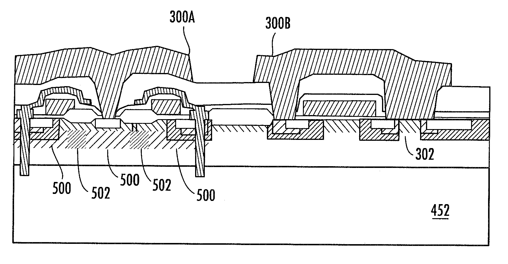
[0029]A first embodiment is depicted in the cross sections of FIGS. 3-10. FIG. 3 depicts a structure including a semiconductor substrate 50, for example silicon, gallium arsenide, silicon carbide, gallium nitride, etc., heavily doped to an N-type conductivity (N+++), for example with arsenic to a concentration of about 1E18 to 1E20 atoms / cm3. The semiconductor substrate 50 is (or will subsequently be) configured such that the depicted region will provide its output to the power converter inductor to provide a device switched node. An N-type epitaxial (epi) layer 52 is formed according to techniques known in the art on the silicon substrate to a thickness which is a function of the desired breakdown voltage of the vertical low-side device to be formed in region 54, with the high-side device formed at region 56. For a 30V breakdown voltage for example, the thickness may be in the range of about 2.5 microns to about 5 microns thick, with a doping concentration in the range of between a...

exemplary embodiment 2

[0043]A second embodiment of the invention is depicted in FIGS. 11-15. The formation of this embodiment includes an additional mask from the method of Exemplary Embodiment 1, and serves to widen the overlap of the metal inside the TSC to provide a larger N+ source to P+ body contact area. The additional mask may result in a device with reduced resistance between the high-side device source and the P-body region compared to the device of Embodiment 1. This device further incorporates a Schottky diode which can be formed by contact between a metal source / body of a low-side VDMOS and an N-doped region of the silicon substrate as described below.

[0044]To form this device, a structure similar to that depicted in FIG. 7 can provided, for example using a flow as described for Embodiment 1, possibly with varying mask dimensions, for example when a different voltage rating is required. The mask of FIG. 7 is removed and a blanket conformal dielectric layer 110, for example oxide, is formed ac...

exemplary embodiment 3

[0051]A third embodiment is depicted in FIGS. 16-25. This embodiment forms a lateral N-channel DMOS high-side device and a vertical N-channel vertical DMOS low side device which includes field isolation between devices.

[0052]FIG. 16 depicts a first processing step including a semiconductor substrate 160, such as silicon, gallium arsenide, silicon carbide, or gallium nitride, etc., heavily doped N+++ to achieve a low-contact resistance, with an N-type dopant such as arsenic or phosphorus to provide a heavily doped substrate. An epitaxial layer 162 is formed on the semiconductor substrate 160, and a pad dielectric 164, such as a pad oxide between about 150 Å and about 400 Å is formed on the epi layer. An upper surface of the epi layer is doped through the pad oxide with an N-type dopant to provide NDRIFT implant 166 for the drain of the High-Side device, and a structure similar to that depicted in FIG. 16.

[0053]Next, after the formation of a blanket pad oxide, a blanket nitride is dep...


PUM


Abstract

A voltage converter includes an output circuit having a high-side device and a low-side device which can be formed on a single die (a “PowerDie”). The high-side device can include a lateral diffused metal oxide semiconductor (LDMOS) while the low-side device can include a planar vertical diffused metal oxide semiconductor (VDMOS). The voltage converter can further include a controller circuit on a different die which can be electrically coupled to, and co-packaged with, the power die.

Description

CROSS-REFERENCE TO RELATED APPLICATION[0001]This application claims priority to provisional U.S. Patent Application Ser. No. 61 / 140,610 filed Dec. 23, 2008, and to provisional U.S. Patent Application Ser. No. 61 / 162,232 filed Mar. 20, 2009, the disclosures of which are herein incorporated by reference in their entirety.FIELD OF THE INVENTION[0002]This invention relates to the field of semiconductor devices, and more particularly to power conversion and control structures and their methods of formation.BACKGROUND OF THE INVENTION[0003]Semiconductor devices which provide power converter functionality, for example for altering DC power using a DC to DC (DC-DC) converter, are used in various capacities. For example, input DC power from one or more batteries can be converted to provide one or more power outputs at voltages which can be higher or lower than the input DC voltage. Performing a power conversion function using integrated circuits (IC's) typically requires a control circuit, a...

Claims


Application Information

Patent Timeline
IPC IPC(8): H01L29/78H01L21/50
CPCH01L21/823487H01L27/088H01L2924/1305H01L2924/12032H01L2924/13062H01L2924/1461H01L2924/13055H01L2924/13091H01L2924/3025H01L2924/30107H01L2224/49171H01L2224/48247H01L2224/48137H02M7/003H01L29/7835H01L29/7816H01L29/7806H01L29/7802H01L29/66712H01L29/66696H01L29/0692H01L29/0696H01L29/1083H01L29/402H01L29/4175H01L29/41766H01L29/41775H01L29/456H01L29/66659H01L2924/00H01L29/7811H01L21/26513H01L21/823437H01L23/535H01L23/62H01L29/0619H01L29/1095H01L29/66681H01L29/66734H01L29/7813
Inventor HEBERT, FRANCOIS
Owner INTERSIL INC
Why Eureka
Try Eureka