Group iii-v nitride layer and method for producing the same

a nitride layer and group iiiv technology, applied in the direction of polycrystalline material growth, crystal growth process, vacuum evaporation coating, etc., can solve the problem of no suitable process for crystal growth, and achieve high quality, improve the properties of a semiconductor device, and improve the crystallinity

Inactive Publication Date: 2010-07-01
KANAGAWA ACADEMY SCI & TECH +2
View PDF3 Cites 21 Cited by
  • Summary
  • Abstract
  • Description
  • Claims
  • Application Information

AI Technical Summary

Benefits of technology

[0054]According to the present invention, there can be provided a hexagonal Group III-V nitride layer having high quality crystallinity capable of improving the properties of a semiconductor device such as a light emitting element. In particular, according to one aspect of the present invention, there can be provided a hexagonal Group III-V nitride layer having high quality whose nonpolar plane can be utilized for avoiding QCSE, and therefore suitable for a light-emitting device. Furthermore, according to another aspect of the present invention, there can be provided a process for manufacturing a hexagonal Group III-V nitride layer exhibiting high quality crystallinity.

Problems solved by technology

In addition, there have been known no suitable process for such crystal growth.

Method used


Image

  • Group iii-v nitride layer and method for producing the same
  • Group iii-v nitride layer and method for producing the same
  • Group iii-v nitride layer and method for producing the same

Examples


examples

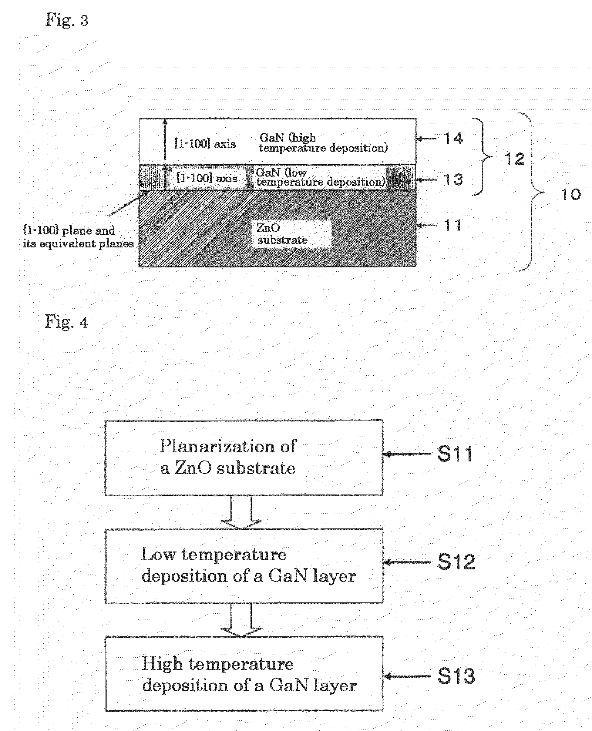
[0202]There will be further detailed the present invention with reference to Examples. In the following description, the flow chart in FIG. 4 is referred as appropriate. First, an example of m-plane growth will be described.

example a-1

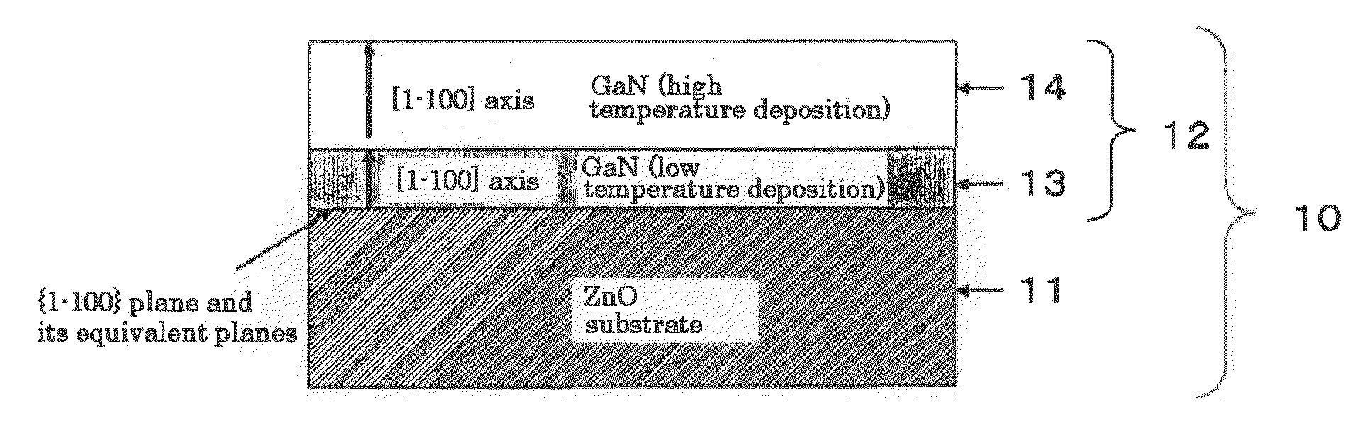
[0203]A ZnO substrate 11 having (1-100) plane as a principal surface was annealed at 1250° C. for 3.5 hrs in the planarization step S11. FIG. 7A shows an atomic force microscopy image after the planarization and, for comparison, FIG. 7B shows an atomic force microscopy image before the planarization. After the planarization, an atomic layer step was observed.

[0204]Then, the above planarized ZnO substrate was introduced into a PLD apparatus, and a GaN layer 13 as a first layer was then deposited in the low temperature deposition step S12 (the first sub-growing step). In the low temperature deposition step S12, the target 32 was made of Ga metal (purity: 99.99%). The target 32 was placed in parallel with (1-100) plane of the ZnO substrate 11. A RF radical source was used as a nitrogen source at 300 W, and a growth pressure was 3×10⁻⁶ Torr.

[0205]A pulse frequency of a pulse laser beam outgoing from a KrF excimer laser 33 was 30 Hz, an irradiation time per 1 pulse was 20 ns, and a laser...

example a-2

[0209]Deposition was conducted as described in Example A-1, except that in the low temperature deposition step S12, a RF radical source as a nitrogen source was used at 400 W, a substrate temperature was 320° C., a growth rate was 53 nm / hr, a growth film thickness was 13 nm; and in the high temperature growth step S13, a laser power at the point of target irradiation was 0.93 W and a substrate temperature was 690° C. The layer was grown to a thickness of about 300 nm. A growth rate was about 300 nm / hr. The resulting layer was evaluated as described in Example A-1. Table 1 shows the growth conditions and Table 2 shows the evaluation results for the film obtained.


PUM

PropertyMeasurementUnit
thicknessaaaaaaaaaa
thicknessaaaaaaaaaa
temperatureaaaaaaaaaa

Abstract

There is disclosed a hexagonal Group III-V nitride layer exhibiting high quality crystallinity capable of improving the properties of a semiconductor device such as a light emitting element. This nitride layer is a Group III-V nitride layer belonging to hexagonal crystal formed by growth on a substrate having a different lattice constant, which has a growth-plane orientation of {1-100} and in which a full width at half maximum b1 of angle dependence of X-ray diffraction intensity in a {1-210} plane perpendicular to the growth-plane upon X-ray incident angle from a direction parallel to the growth-plane satisfies the condition of 0.01°≦b1≦0.5°, or the full width at half maximum b2 of angle dependence of X-ray diffraction intensity in a {0001} plane upon X-ray incident angle from a direction parallel to the growth-plane satisfies the condition of 0.01°≦b2≦0.5°.

Description

TECHNICAL FIELD[0001]The present invention relates to a Group III-V nitride layer, more particularly a Group III-V nitride layer exhibiting good crystallinity which can be used in, for example, a light-emitting device.BACKGROUND ART[0002]With intense research and developmental attempts for Group III-V nitride semiconductor represented by InxAlyGa(1-x-y)N (0≦x≦1, 0≦y≦1, 0≦x+y≦1), there has been exponentially improved a luminous efficiency of a light-emitting device such as a light-emitting diode and a laser diode using such a semiconductor.[0003]InxAlyGa(1-x-y)N represented by GaN belongs to hexagonal crystal and is commonly formed on c-plane of a substrate such as sapphire by epitaxial growth. In a structure where on a GaN layer is deposited a quantum well layer made of InxGa(1-x)N(0<x≦1) mixed crystal as an active layer, it is used or highly expected as a blue and a green LEDs or a layer configuration for a next-generation DVD laser, but due to difference of a lattice constant w...

Claims


Application Information

Patent Timeline
Patent Type & Authority Applications(United States)
IPC IPC(8): H01L29/20H01L21/20
CPCC23C14/0026C23C14/0617C23C14/28C30B23/02C30B23/025C30B29/403H01L21/02403H01L21/0243H01L21/02433H01L21/02458H01L21/0254H01L21/02631H01L21/02658
Inventor FUJIOKA, HIROSHIKOBAYASHI, ATSUSHIHORIE, HIDEYOSHIAMANAI, HIDETAKAMAGAO, SATORU
Owner KANAGAWA ACADEMY SCI & TECH
Why Eureka
Try Eureka