Pulse temporal programmable ultrafast burst mode laser for micromachining

a laser and pulse-time technology, applied in the field of laser micromachining, can solve the problems of “over crater”, reduce the reliability of ic chips, and non-optimal thickness

Inactive Publication Date: 2010-07-15
ELECTRO SCI IND INC
View PDF24 Cites 54 Cited by
  • Summary
  • Abstract
  • Description
  • Claims
  • Application Information

AI Technical Summary

Benefits of technology

[0011]In one embodiment, a laser system is configured for processing a material with a selectively shaped burst of ultrafast laser pulses. The system includes a burst pulse laser configured to emit a burst of three or more laser pulses defined by a selectively shaped burst envelope. The burst pulse laser is further configured to selectively adjust temporal spacing between the three or more laser pulses within the burst envelope and the temporal width of the burst envelope. The system also includes one or more amplifiers configured to amplify the group of three or more laser pulses so as to obtain a desired shape of the burst envelope. In certain embodiments, the burst pulse laser includes a laser source configured to emit a train of laser pulses, and an optical modulator that receives the train of laser pulses. The optical modulator is configured to amplitude modulate the train of laser pulses so as to generate the burst of three or more laser pulses defined by the selectively shaped burst envelope.

Problems solved by technology

Use of a traditional Gaussian-shaped laser pulse having a 5-20 nanosecond pulse width and a sloped, gradually rising front edge in link processing tends to cause an “over crater” in the passivation layer, especially if its thickness is too large or is uneven.
Over cratering reduces the reliability of IC chips.
Difficulty in maintaining wafer-level process control of the passivation layer during IC fabrication may result in non-optimal thickness and poor cross-wafer or wafer-to-wafer thickness uniformity.
However, generating a pulsed laser from a CW light beam is fairly inefficient, and thus requires more amplification.
Because such a low peak-power signal may be influenced by noise, which causes pulse-to-pulse instability, the two modulators are preferably synchronized to maintain pulse stability and energy stability, thereby adding further complexity and cost.
However, the 1 μm and 1.3 μm laser wavelengths with pulse widths in the nanosecond range have disadvantages.
For example, the energy coupling efficiency of such infrared (IR) laser beams into a highly electrically conductive metallic link is relatively poor.
Further, the practical achievable spot size of an IR laser beam for link severing is relatively large and limits the critical dimensions of link width, and link pitch.
Such a conventional link processing laser pulse creates a large heat affected zone (HAZ) that could deteriorate the quality of the device that includes the severed link.
Increased laser pulse energy increases the damage risk to the IC chip, including irregular or over sized opening in the overlying passivation layer, cracking in the underlying passivation layer, damage to the neighboring link structure and damage to the silicon (Si) substrate.
However, using laser pulse energy within a risk-free range on thick links often results in incomplete link severing.
However, the high peak power of a single ultrafast pulse may easily damage the underlying Si substrate, which is unacceptable in many applications.
A problem with using a train of ultrafast pulses is that many commercially available ultrafast lasers that use a pulse picker have pulse repetition rates in the kilohertz range.
Such a repetition rate may be difficult to apply to links because stage movement is typically approximately 400 mm / s such that the laser spot may move off a targeted link in less than approximately 500 nanoseconds.
However, the envelope of a burst of pulses is not capable of being changed, which limits use of the system in various micromachining applications.
In addition, the solution provided by Achim Nebel et al. is large and costly.

Method used


Image

  • Pulse temporal programmable ultrafast burst mode laser for micromachining
  • Pulse temporal programmable ultrafast burst mode laser for micromachining
  • Pulse temporal programmable ultrafast burst mode laser for micromachining

Examples


Embodiment Construction

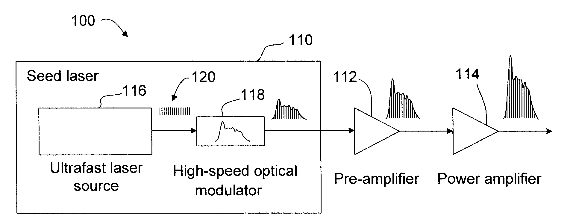
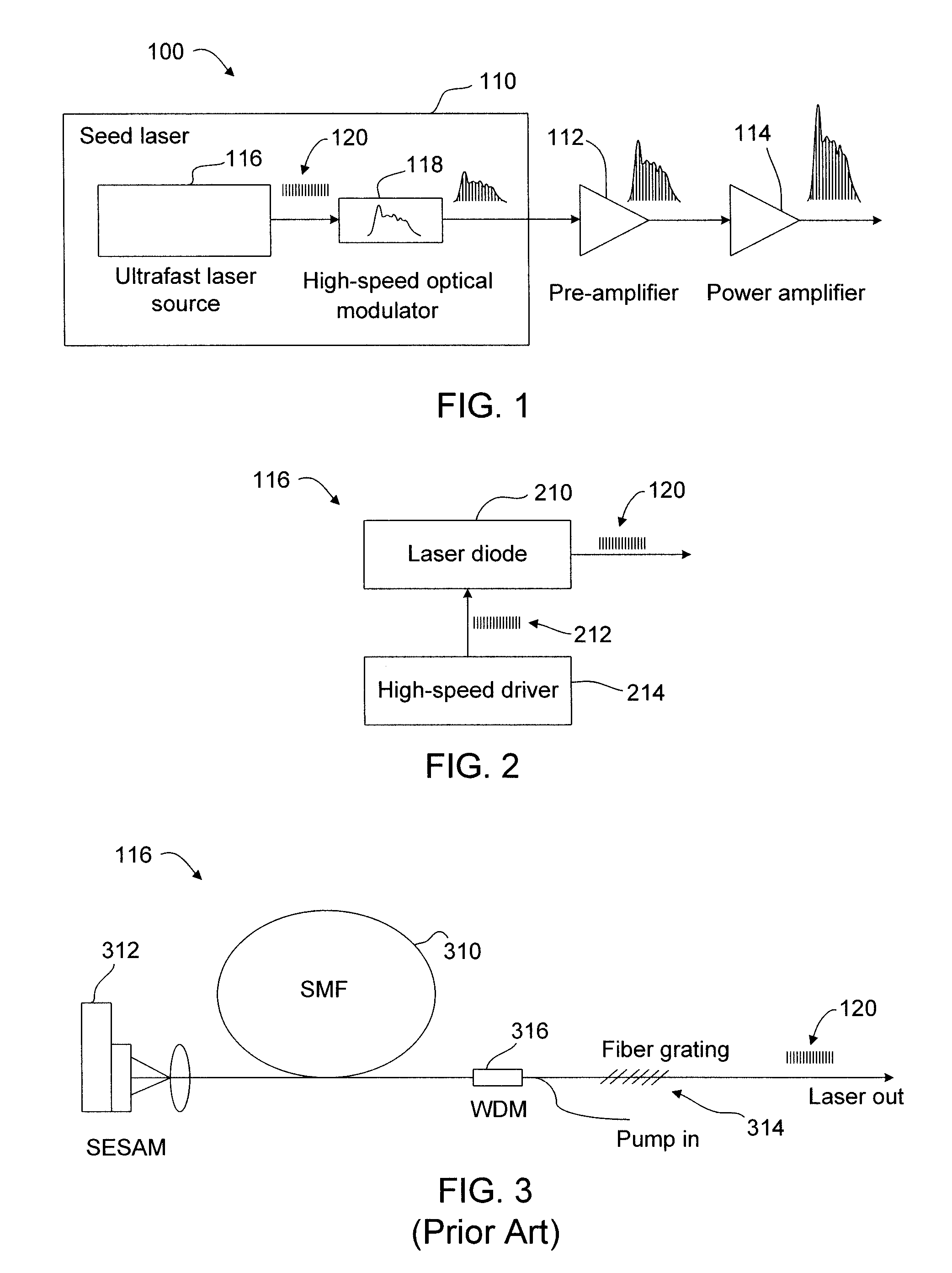
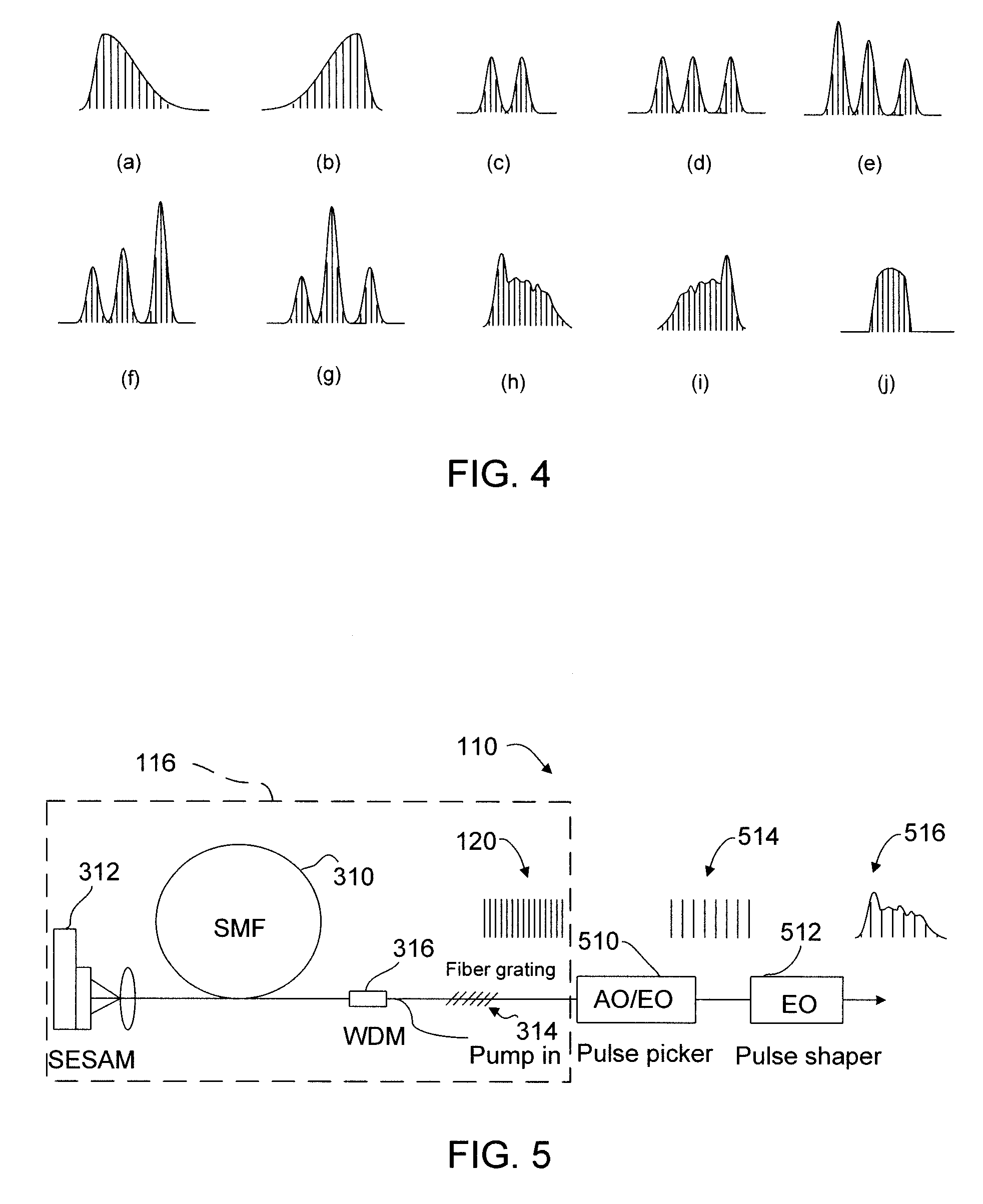
[0023]A laser processing system according to one embodiment generates ultrafast laser pulses with a temporal programmable burst mode. A burst pulse laser includes a high repetition rate ultrafast laser configured to deliver a pulse train with each pulse in the train having an independently controlled amplitude. The respective amplitudes of each ultrafast pulse in a group or “burst” of pulses, along with the spacing between pulses, define a “burst envelope.” In addition to independently controlling the amplitude of each ultrafast pulse in a burst of pulses, the system may also provide selective control of spacing between each ultrafast pulse and / or the overall temporal width of the burst envelope. Thus, the system provides selective shaping of the burst envelope for particular laser processing applications. Because each ultrafast pulse within the group of pulses may have a temporal width in a picosecond range, or even a femtosecond range, the laser system may be used, for example, fo...


PUM

PropertyMeasurementUnit
rise timeaaaaaaaaaa
rise timeaaaaaaaaaa
wavelengthsaaaaaaaaaa

Abstract

A laser processing system provides a burst of ultrafast laser pulses having a selectively shaped burst envelope. A burst pulse laser includes a high repetition rate ultrafast laser to deliver a pulse train with each pulse in the train having an independently controlled amplitude. The respective amplitudes of each ultrafast pulse in a group define a “burst envelope.” In addition to independently controlling the amplitude of each ultrafast pulse within the burst envelope, the system may also provide selective control of spacing between each ultrafast pulse and/or the overall temporal width of the burst envelope. Thus, the system provides selective shaping of the burst envelope for particular laser processing applications.

Description

TECHNICAL FIELD[0001]The present disclosure relates to laser micromachining. In particular, the present disclosure relates to laser systems and methods that use a burst of ultrafast laser pulses.BACKGROUND INFORMATION[0002]After manufacture of a semiconductor memory array chip is complete, integrated circuit (IC) patterns on an exposed surface of the chip are sealed with an electrically insulating layer of passivating material. Typical passivating materials include resins or thermoplastic polymers such as, for example, polyimide. The purpose of this final “passivation” layer is to prevent the surface of the chip from reacting chemically with ambient moisture, to protect the surface from environmental particulates, and to absorb mechanical stress. Following passivation, the chip is mounted in an electronic package embedded with metal interconnects that allow probing and functional testing of the memory cells. When one of many redundant memory cells is determined to be faulty, the cel...

Claims


Application Information

Patent Timeline
Patent Type & Authority Applications(United States)
IPC IPC(8): H01S3/10H01S5/12
CPCB23K26/0635H01S3/06758H01S3/2316H01S5/0085H01S5/12H01S2301/08H01S3/2383B23K26/0624
Inventor PENG, XIAOYUANHOOPER, ANDREW
Owner ELECTRO SCI IND INC
Why Eureka
Try Eureka