Charged particle beam device

a beam device and charge technology, applied in the direction of material analysis using wave/particle radiation, instruments, nuclear engineering, etc., can solve the problems of tangled wirings, difficult to finely control equipotential planes,

Inactive Publication Date: 2010-07-22
HITACHI LTD
View PDF23 Cites 13 Cited by
  • Summary
  • Abstract
  • Description
  • Claims
  • Application Information

AI Technical Summary

Benefits of technology

[0014]According to the present invention, it is possible to realize a charged particle beam device that has a sample stage capab...

Problems solved by technology

However, since the voltage of the conductor plate is invariable, an equipotential plane is uniquely fixed by a height of the conductor plate and a gap between the sample and itself, and therefore it is difficult to control the equipotential plane finely, to correct the electric field distortion as far a...

Method used


Image

  • Charged particle beam device
  • Charged particle beam device
  • Charged particle beam device

Examples


first embodiment

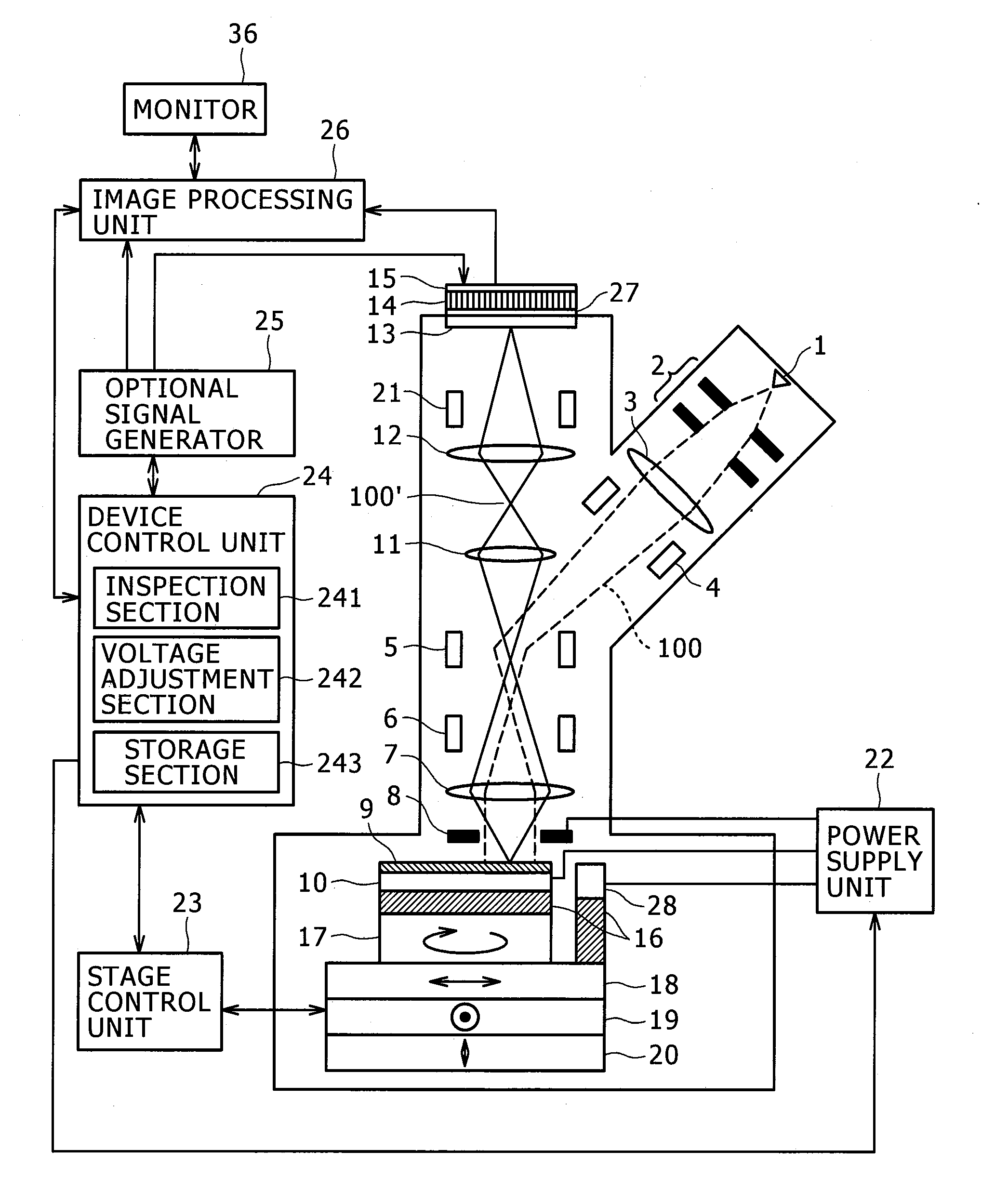
[0041]An inspection device that is according to a first embodiment of the present invention will be explained referring to FIG. 1 to FIG. 10. First, FIG. 1 shows an inspection device that is according to one embodiment of the present invention, namely an entire configuration of a charged particle beam device. This device roughly consists of an electron beam irradiation optical system, a mirror electron imaging optical system, a stage mechanical system, an electric field control mechanical system, an image detection system, and a control system. However, in this figure, a vacuum pump, its control device, an exhaust pipe, etc. are omitted. The electron beam irradiation optical system includes an electron gun 1, an extraction electrode 2, a condenser lens 3, a deflector 4, means for collimating the beam as main constituents. Although there are cases where various constituents are included in addition to these, their details are omitted. The mirror electron imaging optical system includ...

second embodiment

[0076]Next, another example of performing the observation and inspection of the sample 9 that is performed by the inspection part 241 of the device control unit 24 in the device of the first embodiment will be explained referring to FIG. 11 and FIG. 12.

[0077]First, the operator performs initialization of the inspection conditions by the input operation from the GUI screen of the monitor 36 etc. Step 1101 through Step 1106 of FIG. 11 are the same as Step 901 through Step 906 of FIG. 9 of the first embodiment. The image acquired at Step 1106 is processed in the image processing unit 26, and is subjected to the detection processing to detect the existence / absence of a defect of the sample surface. In this embodiment, the X-stage 18 and the Y-stage 19 are moved little by little from the radius position RO continuously, for example, to the inside in the radial direction (Step 1107). Next, at Step 1108, it is determined whether the inspection position reaches the termination (R=Re), for e...

third embodiment

[0080]Next, an inspection device that is according to a third embodiment of the present invention will be explained, referring to FIG. 13 to FIG. 15. First, FIG. 13 is a sectional view of the sample stage and its vicinity of a charged particle beam device that is according to the third embodiment. It is of the same composition as that of the first embodiment except the stage mechanical system and the voltage application mechanical system, and the view is drawn omitting the X-stage 18 and higher-numbered constituents. An electric field control plate 32 isolated by the insulator 16 is provided in the peripheral part of the sample 9 on the sample holder 10. Furthermore, the electric field control electrode 28 is provided on the X-stage 18 in the vicinity of the electric field control plate 32. To the sample 9 and the sample holder 10, the retarding voltage is applied from the power supply unit 22 through the holder receiver 29. To the electric field control electrode 28, a predetermine...


PUM


Abstract

According to the present invention, a charged particle beam device has an unlimitedly rotatable sample stage and an electric field control electrode for correcting electric field distortion at a sample peripheral part. A voltage is applied to a sample on the unlimitedly rotatable sample stage through a retarding electrode that is in contact with a holder receiver at a rotation center of a rotary stage. An equipotential plane on the electric field control electrode is varied by applying a voltage to the electric field control electrode, and following this the equipotential plane at a sample edge is corrected, which enables the sample to be observed as far as its edge.

Description

CLAIM OF PRIORITY[0001]The present application claims priority from Japanese Patent Application JP 2009-009798 filed on Jan. 20, 2009, the content of which is hereby incorporated by reference into this application.FIELD OF THE INVENTION[0002]The present invention relates to a charged particle beam device, and more specifically to a charged particle beam device suitable for observation and inspection of a semiconductor wafer, a magnetic recording medium used in a hard disk drive, etc.BACKGROUND OF THE INVENTION[0003]As a device for inspecting a foreign substance of the semiconductor wafer, a defect of a circuit pattern thereof, etc., devices using electron beams are being used. In these electron beam inspection device, a scanning electron microscope in which an electron beam is focused in the shape of a point and is scanned has become a main stream. In order that the electron beam inspection device performs inspection with desired resolution and sensitivity while suppressing damages ...

Claims


Application Information

Patent Timeline
IPC IPC(8): G01N23/225
CPCH01J37/04H01J37/20H01J2237/0455H01J2237/153H01J2237/2008H01J37/28H01J37/026H01J2237/1536
Inventor SHIMAKURA, TOMOKAZUHASEGAWA, MASAKI
Owner HITACHI LTD
Why Eureka
Try Eureka