Grid-line-free contact for a photovoltaic cell

a photovoltaic cell and contact technology, applied in the field of grid-line-free contact for photovoltaic cells, can solve the problems of reducing and achieve the effect of increasing the effective area of the photovoltaic cell

Inactive Publication Date: 2010-09-02
GLOBALFOUNDRIES INC
View PDF35 Cites 76 Cited by
  • Summary
  • Abstract
  • Description
  • Claims
  • Application Information

AI Technical Summary

Benefits of technology

[0006]In an embodiment of the present invention, a photovoltaic cell that does not employ a wiring structure on the front side is provided. Absence of a wiring structure on the front side increases effective area of the photovoltaic cell. Electrical contact to the front side of the photovoltaic cell is provided by an array of conductive through-substrate vias, and optionally, an array of conductive blocks located on the front side of the photovoltaic cell. A dielectric liner provides electrical isolation of each conductive through-substrate via from the semiconductor material

Problems solved by technology

However, such gird lines block a significant portion of the front side of the p

Method used


Image

  • Grid-line-free contact for a photovoltaic cell
  • Grid-line-free contact for a photovoltaic cell
  • Grid-line-free contact for a photovoltaic cell

Examples


first embodiment

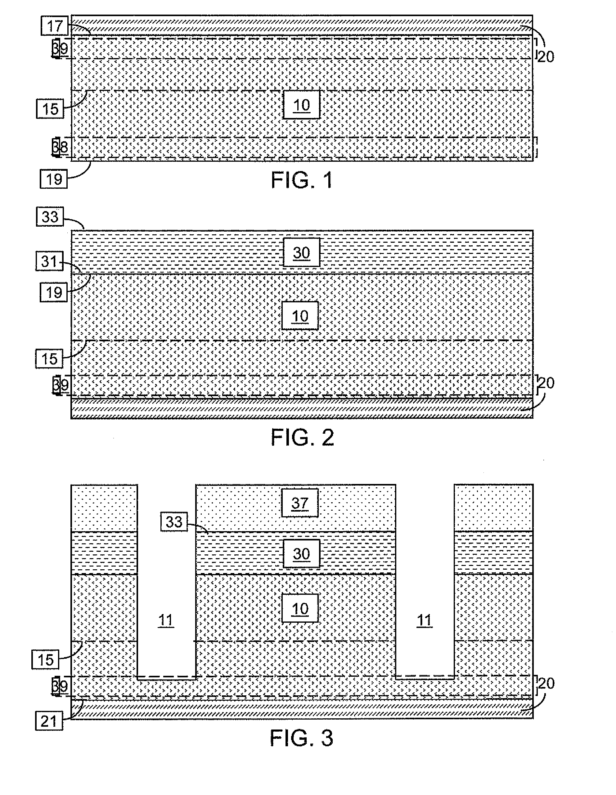
[0021]Referring to FIG. 1, a first exemplary photovoltaic cell structure according to the present invention includes a substrate 10 and an anti-reflective layer 20 located on the front surface 17 of the substrate 10. The substrate 10 includes a photovoltaic material that generates a non-zero electric potential between the front surface 17 and the back surface 19 of the substrate 10 upon irradiation by electromagnetic radiation. The electromagnetic radiation can be in the visible spectrum, ultraviolet range, and / or infrared range.

[0022]The photovoltaic material can be a crystalline material or an amorphous material. The crystalline material can be single crystalline silicon, polycrystalline silicon, germanium, gallium indium, and / or gallium arsenide (GaAs). The amorphous and multicrystalline material can be amorphous silicon, cadmium telluride (CdTe), and / or copper indium diselenide (CuInSe2, or CIS). The photovoltaic material can be in the form of a block, or can be in the form of a...

second embodiment

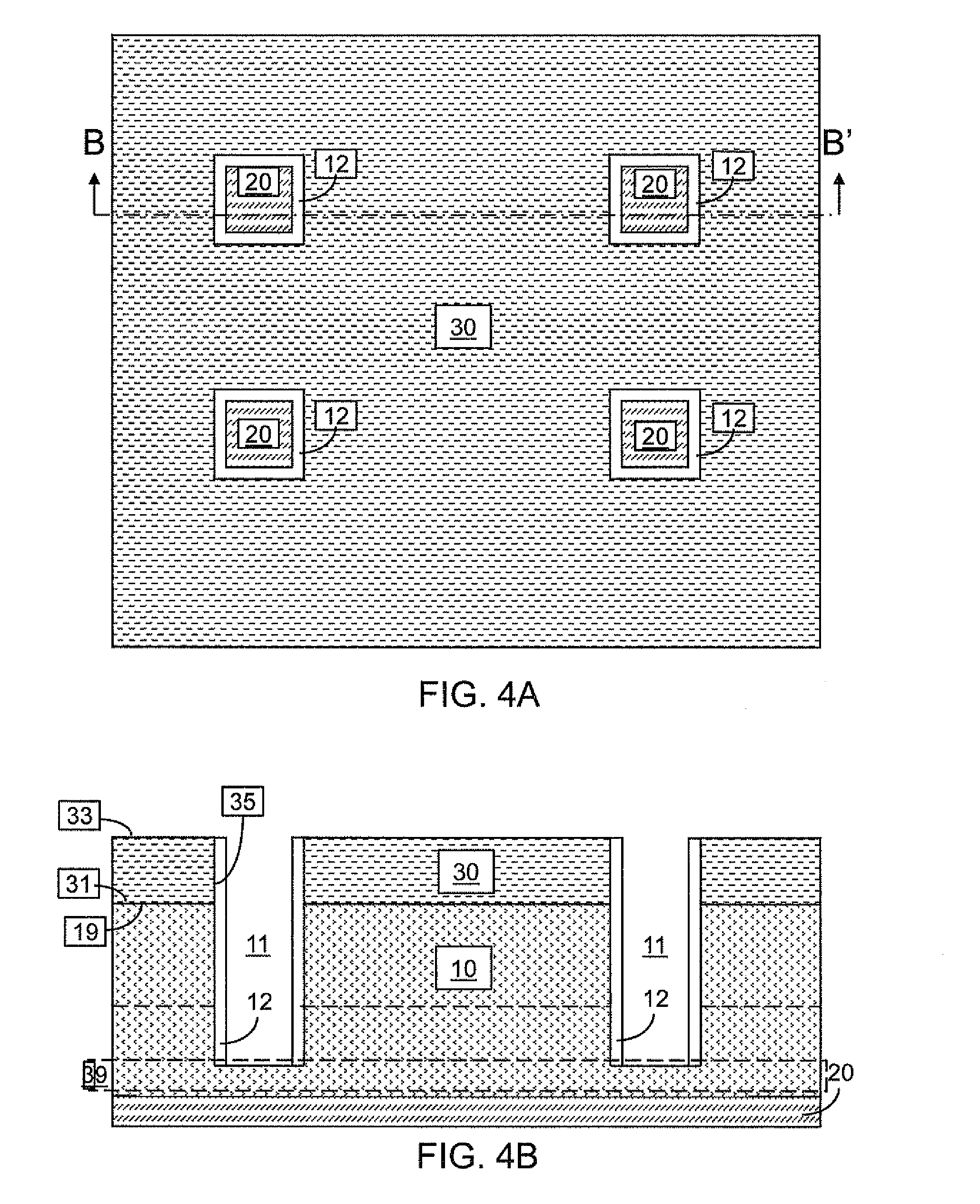
[0048]Referring to FIGS. 10A and 10B, a second exemplary photovoltaic cell structure according to the present invention is derived from the first exemplary photovoltaic cell structure of FIG. 3 by employing a conductive material for the anti-reflective layer 20 and extending the anisotropic etch during the formation of the at least one through-substrate trench 11.

[0049]The anisotropic etch employed to form the at least one through-substrate trench 11 is extended to etch through all of the surface region 39 in the substrate 10. The anisotropic etch can employ an endpoint scheme to stop at the proximal surface 21 of the anti-reflective layer 20. Alternately or additionally, the etch chemistry for the anisotropic etch can be selected to be selective to the material of the anti-reflective layer 20, i.e., to etch only the photosensitive material of the substrate 10 and not to etch the material of the anti-reflective layer 20. In a variation of the second embodiment, the anti-reflective l...

third embodiment

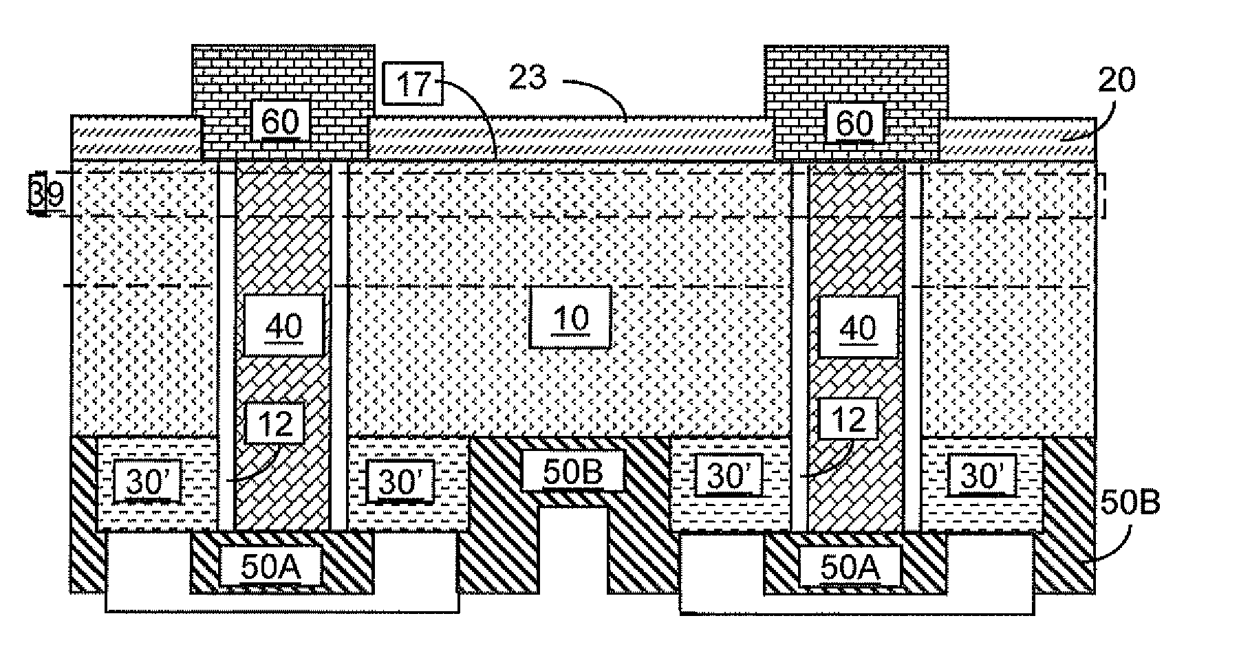
[0053]Referring to FIGS. 13A and 13B, a third exemplary photovoltaic cell structure according to the present invention can be derived from the first exemplary photovoltaic cell structure of FIGS. 9A and 9B or from the second exemplary photovoltaic cell structure of FIGS. 12A and 12B by recessing at least one portion of the substrate 10 from the front side. Specifically, a fourth photoresist 67 can be applied on a distal surface 23 of the anti-reflective layer 20 and lithographically patterned to form at least one opening therein. Preferably, the at least one opening in the fourth photoresist 67 is aligned to the at least one conductive through-substrate via 40 located within the substrate 10. The pattern in the at least one opening in the fourth photoresist 67 is transferred through the anti-reflective layer 20 and into the surface region 39 of the substrate 10 by an etch. The etch may be an anisotropic etch that employs the fourth photoresist 67 as the etch mask.

[0054]The etch form...


PUM


Abstract

Electrical contact to the front side of a photovoltaic cell is provided by an array of conductive through-substrate vias, and optionally, an array of conductive blocks located on the front side of the photovoltaic cell. A dielectric liner provides electrical isolation of each conductive through-substrate via from the semiconductor material of the photovoltaic cell. A dielectric layer on the backside of the photovoltaic cell is patterned to cover a contiguous region including all of the conductive through-substrate vias, while exposing a portion of the backside of the photovoltaic cell. A conductive material layer is deposited on the back surface of the photovoltaic cell, and is patterned to form a first conductive wiring structure that electrically connects the conductive through-substrate vias and a second conductive wiring structure that provides electrical connection to the backside of the photovoltaic cell.

Description

BACKGROUND[0001]The present invention generally relates to structures that provide electrical contacts only from a backside of a multi junction photovoltaic cell in order to increase an effective area of the photovoltaic cell, and methods of manufacturing the same.[0002]A photovoltaic cell is a device that converts light directly into electricity by the photovoltaic effect. Assemblies of photovoltaic cells are used to make solar panels, solar modules, or photovoltaic arrays. A photovoltaic cell can be formed by providing a large area p-n junction in a semiconductor material.[0003]A space charge region is formed around a p-n junction in a photovoltaic cell. Photons that impinge on the space charge region generate at least one electron-hole pair if absorbed by the semiconductor material in the space charge region. The electrons and holes diffuse in opposite directions, thereby accumulating positive charges in the bulk portion of the p-doped material and accumulating negative charges i...

Claims


Application Information

Patent Timeline
IPC IPC(8): H01L31/00H01L31/18
CPCH01L31/0682Y02E10/547H01L31/1804H01L31/02245Y02E10/544Y02P70/50H01L31/022425H01L31/0687
Inventor GUHA, SUPRATIKMARTIN, YVESMOUMEN, NAIMSANDSTROM, ROBERT L.VAN KESSEL, THEODORE G.
Owner GLOBALFOUNDRIES INC
Why Eureka
Try Eureka