Method of manufacturing silicon carbide semiconductor device

a semiconductor device and silicon carbide technology, applied in semiconductor devices, electrical devices, electric discharge tubes, etc., can solve the problems of disadvantageous characteristics of mosfet including silicon carbide substrates, and achieve the effect of low interface state density

Inactive Publication Date: 2010-09-02
SUMITOMO ELECTRIC IND LTD
View PDF13 Cites 23 Cited by
  • Summary
  • Abstract
  • Description
  • Claims
  • Application Information

AI Technical Summary

Benefits of technology

[0013]According to the method of manufacturing a silicon carbide semiconductor device of the present invention, the silicon carbide semiconductor device having low interface state density in the interface region between the gate insulating film and the silicon carbide layer can be obtained.

Problems solved by technology

Meanwhile, as compared with an MOSFET (Metal Oxide Semiconductor Field Effect Transistor) including a silicon substrate, an MOSFET including the silicon carbide substrate is disadvantageous in poor characteristics of a silicon oxide film serving as a gate insulating film, for the following reasons.

Method used


Image

  • Method of manufacturing silicon carbide semiconductor device
  • Method of manufacturing silicon carbide semiconductor device
  • Method of manufacturing silicon carbide semiconductor device

Examples


embodiment

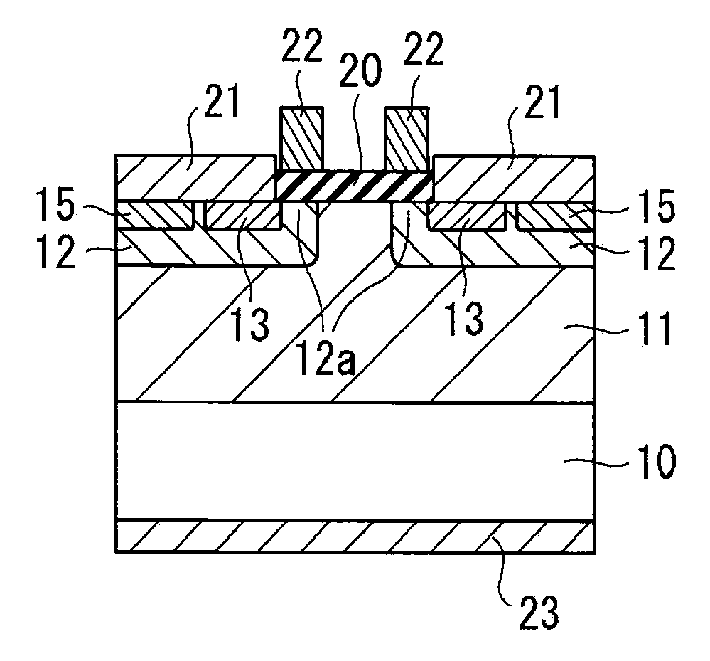
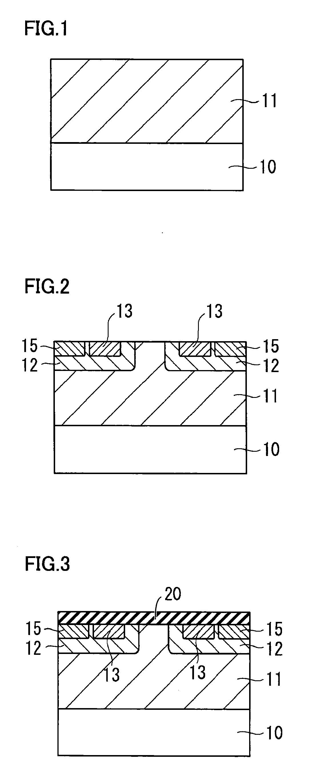
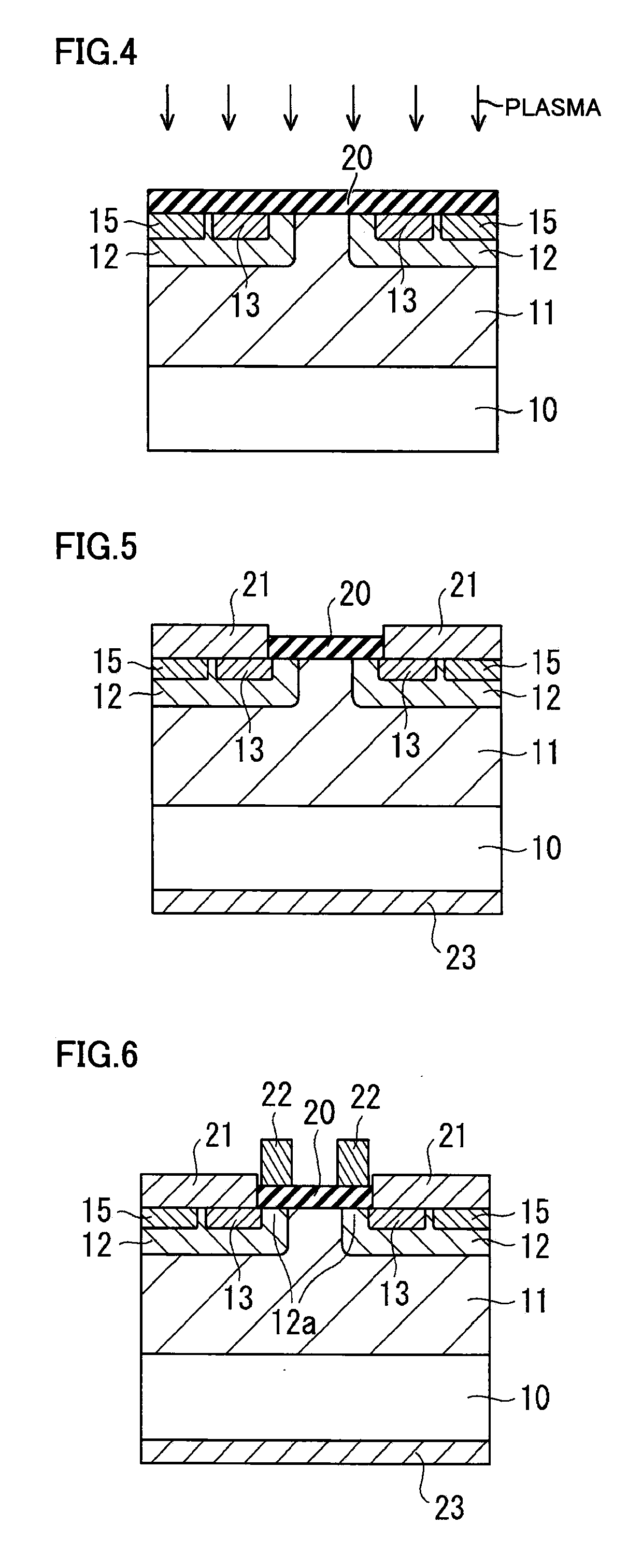
[0023]FIGS. 1 to 6 are cross-sectional views showing steps of manufacturing an MOSFET representing a silicon carbide semiconductor device in an embodiment.

[0024]Though FIGS. 1 to 6 show solely two transistor cells representing a part of a vertical MOSFET, a large number of transistor cells are integrated to configure one vertical MOSFET.

[0025]In the step shown in FIG. 1, an n-type 4H (hexagonal)-SiC (4 represents the number of layers stacked in one period) substrate 10, for example, having a resistivity of 0.02 Ωcm and a thickness of 400 μm, and having a (0001) face at an off angle of approximately 8° in [11-20] direction as a main surface is prepared. Then, using CVD epitaxial growth including in-situ doping, an epitaxially grown layer 11, for example, containing an n-type dopant in a concentration of approximately 5×1015 cm−3 and having a thickness of approximately 10 μm is grown on 4H-SiC substrate 10. An outermost surface of epitaxially grown layer 11 immediately after epitaxial...


PUM

PropertyMeasurementUnit
temperatureaaaaaaaaaa

Abstract

A method of manufacturing a silicon carbide semiconductor device having low interface state density in an interface region between a gate insulating film and a silicon carbide layer is provided. An epitaxially grown layer is grown on a 4H-SiC substrate, and thereafter ion implantation is performed to form a p well region, a source region and a p+ contact region that are ion implantation layers. Thereafter, using thermal oxidation or CVD, the gate insulating film formed by a silicon oxide film is formed on the p well region, the source region and the p+ contact region. Then, plasma is generated using a gas containing N2O, which is the gas containing at least any one of oxygen and nitrogen, so as to expose the gate insulating film to plasma.

Description

TECHNICAL FIELD[0001]The present invention relates to a method of manufacturing a silicon carbide semiconductor device such as an MOSFET, having a gate insulating film low in interface state density.BACKGROUND ART[0002]Semiconductor devices such as a transistor and a diode formed with a silicon carbide substrate (SiC substrate) composed of silicon (Si) and carbon (C) bonded to each other at a composition ratio of 1:1 have been expected to go into actual use as power devices. As silicon carbide is a wide bandgap semiconductor, its breakdown electric field is higher than that of silicon by one order of magnitude. Accordingly, even if a depletion layer at a pn junction or a Schottky junction has a smaller thickness, a high peak inverse voltage can be maintained. Here, as use of the silicon carbide substrate permits smaller thickness of the device and higher doping concentration, implementation of a power device having a low ON resistance, a high withstand voltage, and low loss has been...

Claims


Application Information

Patent Timeline
Patent Type & Authority Applications(United States)
IPC IPC(8): H01L21/04
CPCH01J37/3244H01L21/02164H01L21/02236H01L21/02255H01L21/0234H01L21/049H01L29/7802H01L21/3148H01L21/31658H01L29/1608H01L29/518H01L29/66068H01L21/3147H01L21/18H01L21/3065
Inventor MASUDA, TAKEYOSHI
Owner SUMITOMO ELECTRIC IND LTD
Why Eureka
Try Eureka